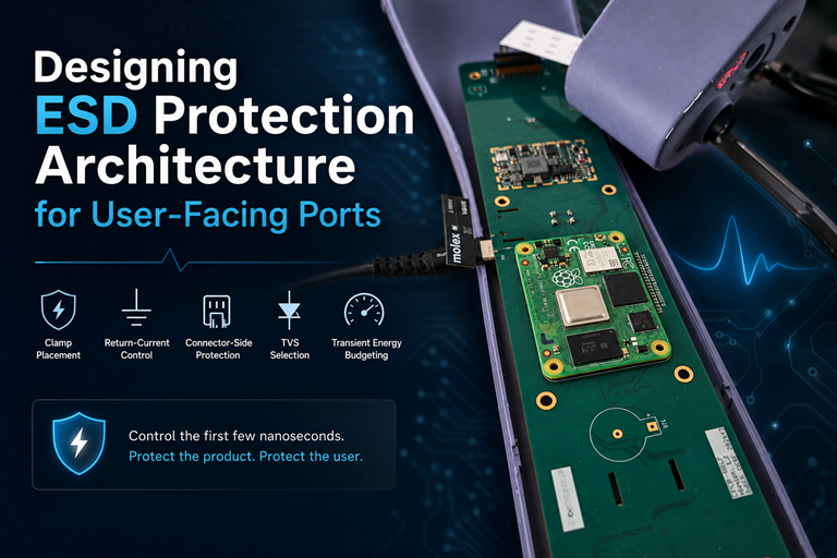
Designing ESD Protection Architecture for User-Facing Ports
Clamp placement, return-current control, connector-side protection, TVS selection, and transient energy budgeting
User-facing ports are where the controlled environment of a product meets the unpredictable outside world.
A PCB inside an enclosure operates with known voltages, controlled impedance, defined signal levels, and carefully planned current paths. The moment a user touches a connector, plugs in a cable, inserts a memory card, connects a charger, or interacts with a button interface, the product is exposed to events that were never part of normal operation.
One of the most common examples is electrostatic discharge (ESD).
A user walking across a carpet, touching a metal object, and then connecting a cable can introduce a very fast transient event. The voltage can be extremely high, but the more challenging part is not only the voltage level.
It is the speed.
An ESD event rises much faster than most system-level protections can react. The transient energy attempts to find the shortest path through the product, and if the PCB does not provide an intentional path, it will create one itself.
This is where many hardware failures begin.
The problem is usually not that the design completely missed ESD protection. Most modern designs include a TVS diode or protection component.
The problem is that the protection architecture was treated as a component selection task instead of a current-flow problem.
At Hoomanely, ESD protection is viewed as energy steering architecture.
The goal is not simply to absorb a transient.
The goal is to decide:
- where the transient enters,
- where the energy is diverted,
- which ground path carries the current,
- and which sensitive circuits never experience the event.
A strong ESD design does not make the transient disappear.
It gives the transient a controlled path.
The Protection Boundary Starts at the Connector
The connector is the first point where the outside world interacts with the PCB.
That makes it the first protection boundary.
One of the most common PCB mistakes is placing ESD components near the IC because the IC is considered the sensitive element.
Electrically, this looks logical.
Physically, it is often too late.
An ESD event entering through a connector can travel several centimeters across the PCB before reaching the protection device. During this journey, the transient current can already couple into:
- nearby signal traces,
- power planes,
- sensitive sensor circuits,
- communication interfaces,
- processor pins.
The protection device may still clamp the voltage, but the unwanted current has already travelled through the system.
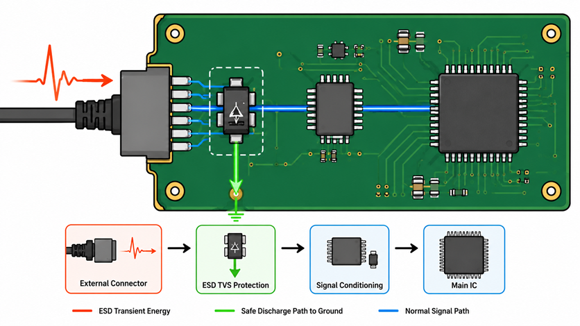
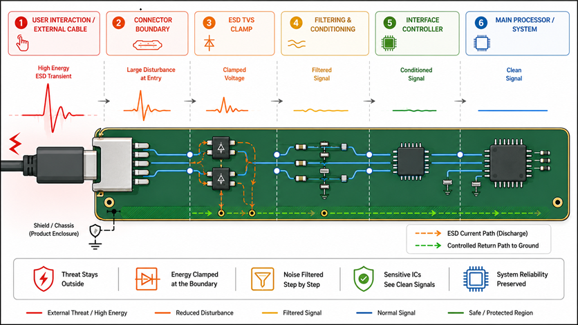
The preferred architecture is:
Connector → ESD Clamp → Filter/Conditioning → Internal Circuit
The ESD protection should sit close to the connector pins.
The distance between the connector and the clamp directly affects the inductance of the discharge path.
Even a few millimeters can matter during a fast transient.
The shorter the path, the lower the unwanted voltage developed across the protection connection.
A TVS diode that is electrically close but physically connected through a long thin trace is not truly close.
The PCB geometry becomes part of the protection circuit.
Clamp Placement Determines the First Current Path
When an ESD event occurs, current does not politely follow the schematic.
It follows impedance.
At high frequencies, a small inductance can create a significant voltage difference.
This means the placement of the clamp decides where the first transient current flows.
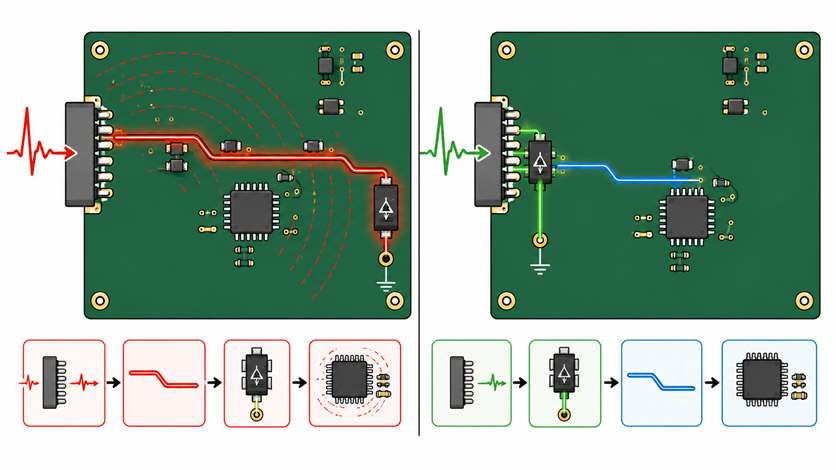
Consider two designs.
In the first design:
Connector → long trace → TVS diode → ground
The transient enters the PCB and travels before reaching protection.
The trace itself becomes part of the transient path.
In the second design:
Connector → TVS diode → short ground connection
The transient is immediately diverted away from sensitive areas.
The second design creates a controlled boundary.
Good clamp placement usually follows a few practical rules:
- Place TVS devices as close as possible to the connector pins.
- Keep the connection between connector and TVS short.
- Avoid routing protected signals through large PCB areas before clamping.
- Place the return connection close to the TVS device.
- Avoid long vias or narrow traces in the discharge path.
The protection component is only one part of the solution.
The copper around it decides its real performance.
Return-Current Control Is the Hidden Part of ESD Design
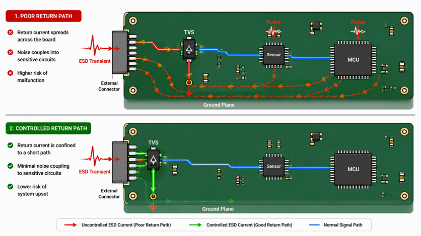
Many ESD failures happen because designers focus only on the discharge path and ignore the return path.
A transient current must return somewhere.
If the return path is not intentional, the current searches for alternatives.
Those alternatives may include:
- digital ground planes,
- communication shields,
- processor ground pins,
- sensor references,
- cable shields.
This is how a connector-level event becomes a system-level failure.
For example, a USB connector may have a TVS diode connected to ground. But if that ground connection travels through a narrow trace across the PCB before reaching the main ground structure, the transient current creates a voltage rise along that path.
Sensitive circuits connected to the same ground reference can experience this disturbance.
A good ESD architecture separates:
High transient current paths
from
Sensitive functional ground paths
The return current should have a short, low-inductance route.
This usually means:
- short ground connection from TVS to reference plane,
- direct connection to chassis ground where applicable,
- controlled separation between noisy discharge currents and sensitive circuits,
- avoiding unnecessary sharing of transient return paths.
The question is not only:
"Where does the ESD current enter?"
The better question is:
"Where does the ESD current leave?"
Choosing the Right TVS Device Requires Energy Understanding
Selecting a TVS diode is often reduced to checking the voltage rating.
But ESD protection requires understanding the complete transient environment.
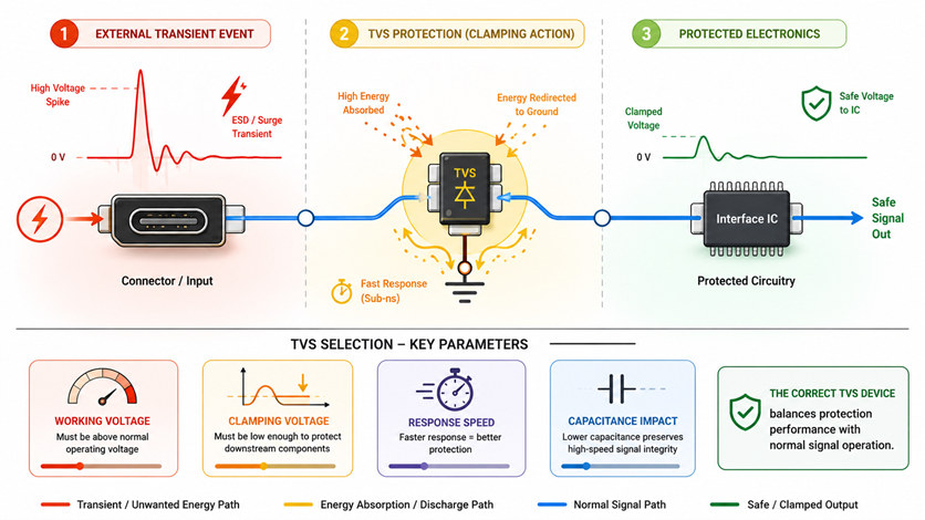
A TVS device must satisfy several conditions:
The working voltage must be higher than the normal operating voltage.
The clamping voltage must remain safe for the protected component.
The response time must be fast enough for the transient.
The device must handle the expected transient energy.
A device with excellent clamping characteristics but poor energy capability may fail after repeated events.
A device with high energy capability but excessive clamping voltage may protect itself while damaging the downstream IC.
The selection process should consider:
- normal signal voltage,
- maximum acceptable clamp voltage,
- expected ESD level,
- pulse duration,
- repetitive event exposure,
- leakage requirements.
For high-speed interfaces, another factor becomes important:
The protection device itself must not damage signal integrity.
Large capacitance TVS devices may protect well but introduce:
- signal attenuation,
- slower edges,
- communication instability.
The protection component must fit the electrical behaviour of the interface.
Protection is not separate from functionality.
It is part of the interface design.
Transient Energy Budgeting Before Choosing Protection
A good ESD architecture begins with an energy budget.
The question is:
How much energy can this protection path safely handle?
The transient source provides energy.
The protection network absorbs and redirects that energy.
The PCB structure determines where the remaining disturbance travels.
Without understanding this balance, component selection becomes guesswork.
For a user-facing port, the design team should understand:
- maximum expected transient severity,
- number of repeated events,
- available grounding paths,
- enclosure connection,
- cable characteristics,
- sensitive components nearby.
A connector connected directly to a processor communication pin has a different protection challenge compared to a connector connected through an isolated interface device.
The architecture changes the energy flow.
The best designs reduce the energy before it reaches sensitive silicon.
They do not depend on the IC surviving the event.
Protection Components Should Not Become Noise Sources
Another common mistake is adding protection without considering normal operation.
A TVS diode, filter, and protection network can affect:
- signal rise time,
- communication timing,
- analog accuracy,
- leakage current,
- standby power.
This becomes especially important in low-power products.
A protection device with high leakage may pass ESD testing but create battery-life problems.
A high-capacitance device may protect a communication line but reduce interface margin.
The protection design must balance:
- transient performance,
- signal integrity,
- power consumption,
- product lifetime requirements.
The best protection network is invisible during normal operation and active only when needed.
Designing ESD Protection That Can Be Debugged
ESD problems are often discovered late during certification testing.
At that stage, debugging time becomes expensive.
A PCB designed with future tuning in mind makes this process easier.
Useful practices include:
- keeping optional TVS footprints,
- allowing different protection devices during validation,
- providing accessible measurement locations,
- maintaining clear separation between protected and unprotected regions,
- documenting the intended transient path.
A good PCB should make the protection strategy obvious.
Future engineers should be able to look at the board and understand:
"This is where the external energy enters."
"This is where it is redirected."
"This area remains protected."
Design intent is part of reliability.
Hoomanely View: ESD Protection Is About Controlling the First Few Nanoseconds
Most hardware failures caused by ESD are not because the product cannot survive a large voltage.
They happen because the first few nanoseconds were uncontrolled.
The transient found an unexpected path.
The ground return was too long.
The clamp was too far away.
The connector boundary was ignored.
The sensitive circuit saw energy that should never have reached it.
At Hoomanely, ESD protection is considered a physical architecture problem.
The component matters.
But the placement matters more.
The current path matters even more.
A good design answers one simple question:
When an external transient enters the product, do we know exactly where the energy goes?
If the answer is yes, the system is protected.
If the answer is uncertain, the PCB is relying on luck.
Final Thoughts
User-facing ports are the most exposed parts of any electronic product.
They connect controlled hardware to uncontrolled environments.
A reliable ESD protection architecture does not start with selecting a TVS diode.
It starts with understanding the boundary.
Place protection at the connector.
Control the return current.
Budget the transient energy.
Choose protection devices that match both electrical and physical requirements.
Design the PCB so the transient follows the path you created, not the path it discovers.
Because in real hardware, ESD protection is not about blocking the event.
It is about giving the event nowhere else to go.