Designing PCB Stack-Up Standards for Controlled Impedance Across Revisions
A controlled-impedance PCB is easy to get right once.
The difficult part is getting it right again six months later, when the board has a different connector, a new processor, a changed power section, a second PCB supplier, and someone opens the original layout and says, “We can keep the same stack-up and just move these traces.”
That is exactly where impedance-controlled designs start to drift.
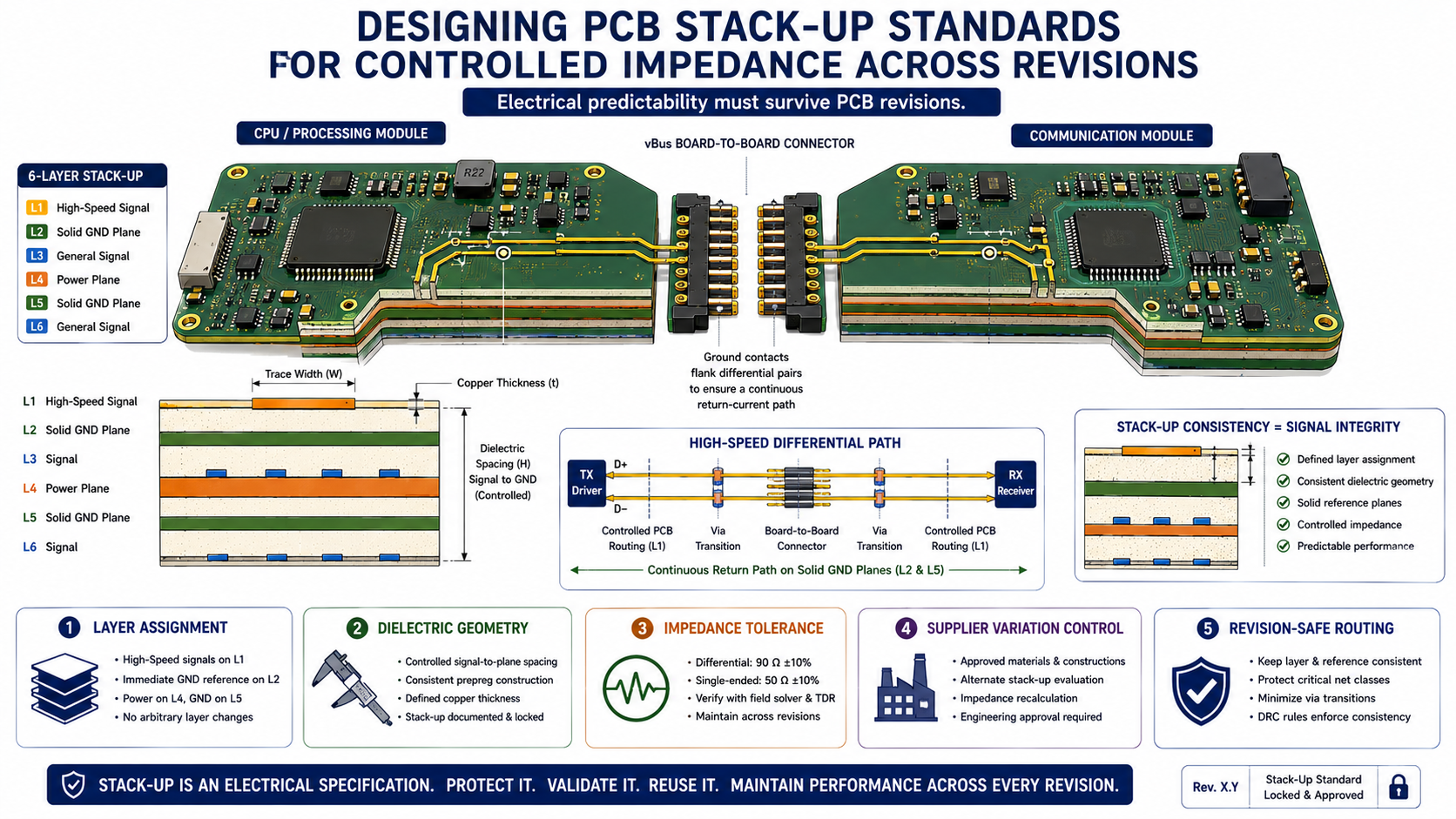
At Hoomanely, the vBus architecture is built around modularity. CPU SoMs, Power SoMs, Communication modules, and peripheral boards are expected to remain electrically compatible even as individual boards evolve. That makes PCB stack-up a system-level standard rather than a one-time layout decision. vBus assigns dedicated high-speed lanes, maintains defined reference relationships, and treats signal integrity as part of the architecture rather than something to repair during a respin.
The practical rule is simple:
A revision should be allowed to change the circuit without silently changing the transmission line.
The real problem: impedance changes without a routing change
Design teams usually think of controlled impedance as a trace-width problem.
It isn't.
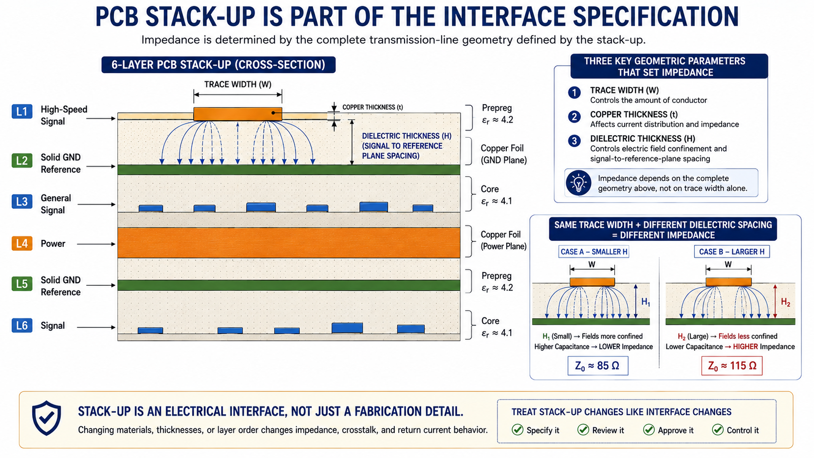
Impedance is determined by the complete transmission-line geometry: trace width, copper thickness, distance to the reference plane, dielectric properties, soldermask effects, and the geometry around neighbouring conductors.
Change any of those and the same 50 Ω trace is no longer necessarily 50 Ω.
This becomes particularly dangerous in a modular system. A vBus communication lane can leave one module, cross a board-to-board connector, enter another PCB, and continue into a receiver. The logical net has not changed, but its physical environment can change several times along that path. Hoomanely's vBus signal-integrity approach therefore treats connectors, stack-ups, return paths, and routing as one transmission-line problem.
That leads to our first stack-up rule:
The stack-up is part of the interface specification.
Not a fabrication preference. Not a screenshot attached to an old project.
1. Layer assignment comes before component placement
When a new vBus PCB starts, we do not begin by deciding where the processor goes and then work out where the high-speed signals can fit.
We assign signal classes to layers first.
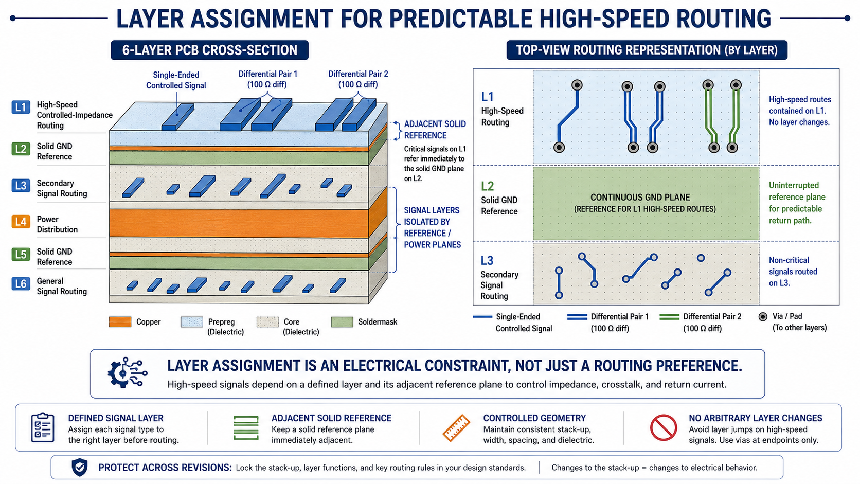
A typical structure reserves dedicated layers for high-speed routing, keeps solid reference planes adjacent to those layers, and ensures that critical signals do not have to cross an uncontrolled reference transition. The exact layer count can change with board complexity, but the electrical relationship must remain stable.
For example:
- High-speed single-ended and differential signals stay on defined impedance-controlled layers.
- Each critical signal layer has an immediately adjacent reference plane.
- Ground is preferred as the reference because it provides a predictable return path.
- Power planes are not casually treated as interchangeable references.
- Plane transitions are avoided unless the return path is deliberately engineered.
In vBus designs, the reference plane is not simply “somewhere below the trace.” We minimise the signal-to-plane distance because that geometry controls field confinement, crosstalk, and achievable impedance.
This also makes the design easier to revise. When an engineer knows that Layer 1 is always a controlled-impedance outer layer and Layer 3 is always a referenced internal signal layer, moving a connector or swapping a processor does not require rediscovering the electrical rules.
2. Dielectric consistency matters more than the laminate name
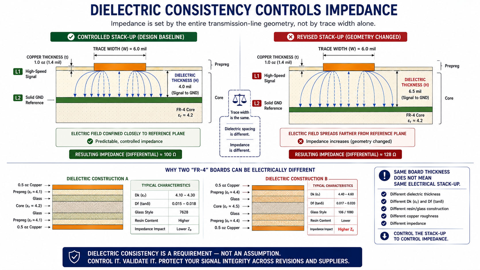
“FR-4” is not a complete stack-up specification.
Two boards can both be sold as FR-4 and still produce noticeably different electrical behaviour because resin content, glass weave, cured thickness, dielectric constant, copper thickness, and fabrication process are not identical.
For high-speed vBus interfaces, the dielectric environment is part of the signal path. Hoomanely has specifically treated dielectric variation and glass-weave effects as signal-integrity concerns; a differential pair can experience different local dielectric environments across the weave, creating skew and common-mode conversion.
That is why a revision-safe stack-up should define more than:
“4-layer FR-4, 1.6 mm.”
The controlled parameters are the dielectric thickness between each signal and its reference, the intended material system, copper thickness, and the electrical properties used by the impedance calculation.
We also avoid changing prepreg construction simply to meet an overall mechanical thickness target. A board can remain 1.6 mm thick while the electrical geometry underneath a high-speed trace changes enough to move its impedance outside the intended window.
Mechanical thickness may stay constant while electrical thickness changes.
That distinction is critical.
3. Impedance tolerance must be designed, not assumed
Every controlled-impedance net should have a declared target.
For vBus high-speed interfaces, that commonly means a defined single-ended or differential impedance such as 50 Ω or 100 Ω, depending on the interface. Hoomanely's routing methodology explicitly uses these impedance targets rather than treating high-speed traces as ordinary PCB tracks.
But the nominal number is only half of the requirement.
The stack-up specification must also define the acceptable tolerance and who owns that tolerance:
Designer → PCB fabricator → finished board.
A calculated 50 Ω line is meaningless if the fabricator interprets the geometry differently, changes dielectric thickness, or substitutes a materially different construction.
For that reason, we treat impedance tolerance as a manufacturing requirement, not merely a CAD property. The impedance target, tolerance, test method, and controlled layers belong in the fabrication documentation.
This prevents a common failure mode: a layout is released with “50 Ω differential” written in the net class, while the manufacturing package contains no enforceable stack-up requirement.
4. Supplier variation is a design variable
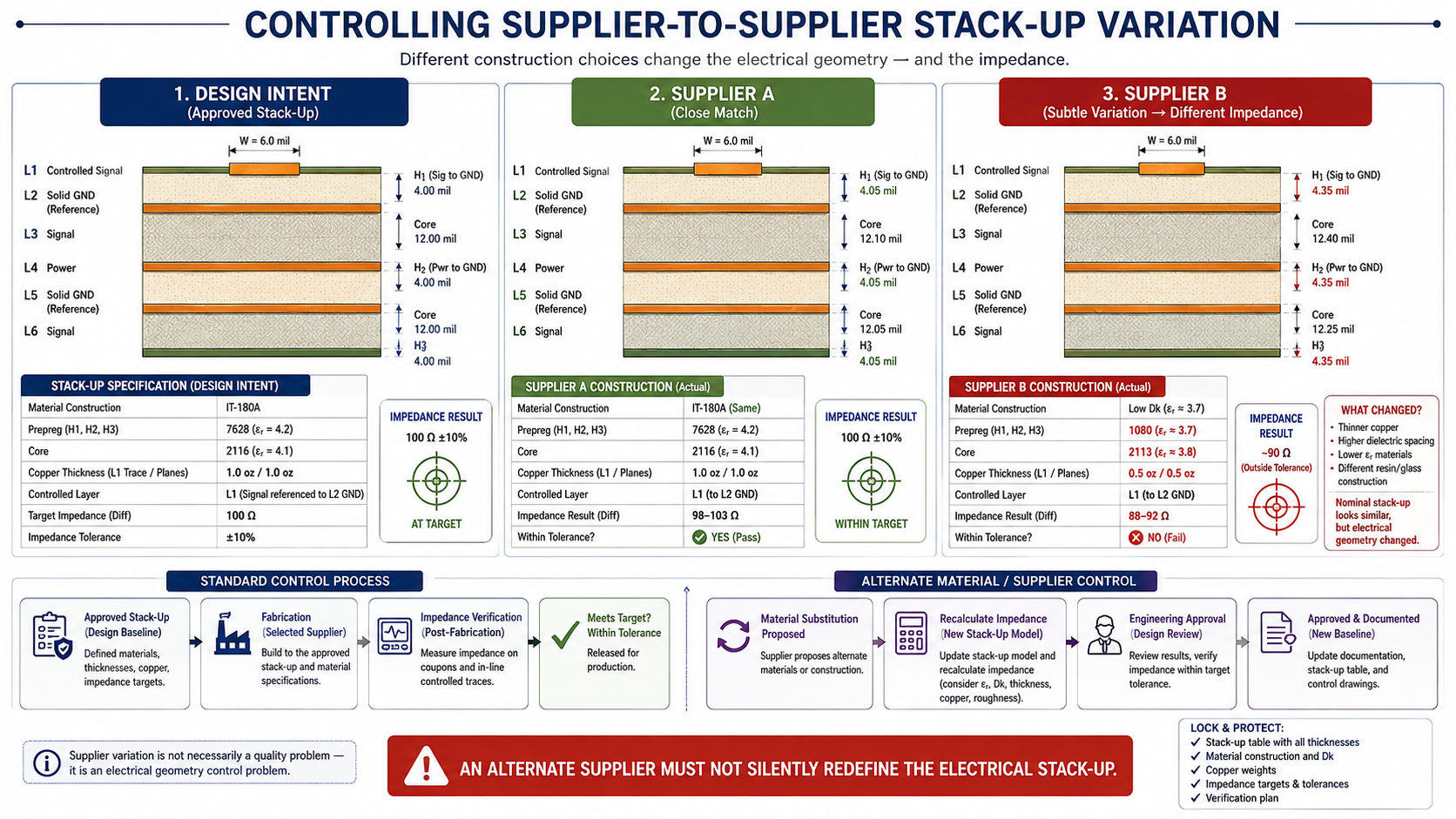
A stack-up that works perfectly with one fabricator can move outside its intended impedance range at another supplier.
The problem is often not supplier quality. It is supplier construction.
Different PCB houses may use different glass styles, resin contents, copper foil thicknesses, or standardised prepreg constructions to achieve the requested board thickness. Hoomanely's vBus approach already treats manufacturing capability as part of the design-rule framework; PCB rules are tied to actual fabricator capabilities rather than theoretical limits.
We apply the same philosophy to stack-up.
A production stack-up should have:
- A preferred material construction.
- An approved alternate construction.
- Controlled dielectric thicknesses for impedance-critical layers.
- Defined copper thickness after fabrication.
- A documented impedance target and tolerance.
- A clear process for approving substitutions.
The important part is that an alternate supplier does not get permission to redesign the electrical stack-up implicitly.
Any substitution that changes the signal-to-plane geometry must trigger impedance recalculation before fabrication.
5. Revision-safe routing rules
This is where stack-up standards become genuinely useful.
A revision-safe PCB should make it difficult for an engineer to accidentally break the electrical architecture.
Our rules for a vBus-style design are straightforward.
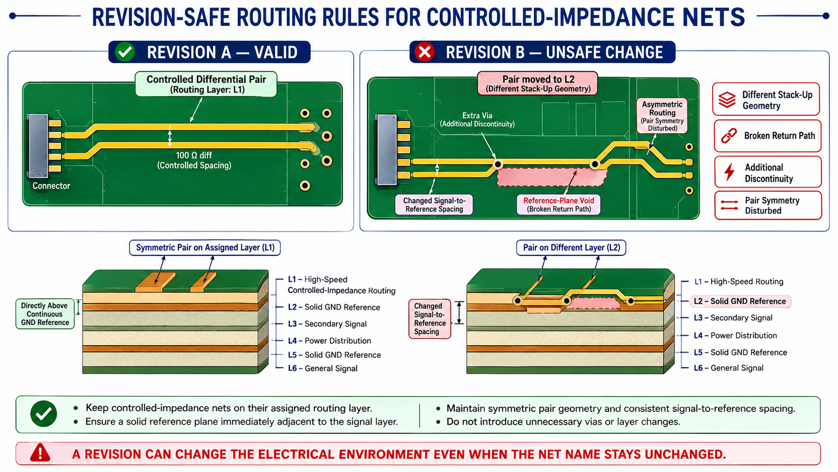
Do not change the layer used by a controlled-impedance net without re-validation.
A differential pair routed on Layer 1 should not casually move to Layer 3 because Layer 3 “has more space.” The trace-width rule is different, the reference distance may be different, and the via transition introduces another discontinuity.
Do not change the reference plane under an existing high-speed route.
If a revision introduces a plane void, split, connector keep-out, or new power island under the route, the return path has changed even though the trace itself has not.
This is why vBus designs favour solid, unified ground planes rather than physically splitting analogue and digital ground beneath routing.
Do not change the stack-up to solve routing congestion.
If routing no longer fits, change the routing architecture or the board layer count intentionally. Changing dielectric thickness or copper construction to recover a small amount of routing space can invalidate every existing impedance calculation.
Do not resize a controlled trace manually.
Trace width should come from the stack-up-specific rule set. If the stack-up changes, the rule should change centrally and the affected nets should be rechecked.
Keep high-speed paths structurally repeatable.
For differential pairs, symmetry and return-path continuity matter more than simply achieving equal total length. Hoomanely's vBus routing practices explicitly account for pair symmetry, fibre-weave effects, adjacent reference planes, and connector transitions.
6. The stack-up must survive the connector
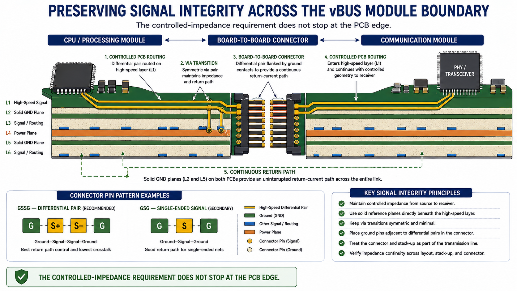
A vBus module can have an excellent PCB stack-up and still fail at the board-to-board connector.
The connector is another transmission-line transition.
That is why vBus pin assignment places return paths next to high-speed signals: GSG for single-ended signals and GSSG for differential pairs. The intent is to preserve the electrical environment as the signal moves from PCB copper into the connector and back into the next PCB.
The stack-up standard therefore cannot stop at the PCB edge.
It must define how Layer 1 or internal-layer routing approaches the connector, where reference copper is retained or removed, how vias are arranged, and how much discontinuity is acceptable.
7. Validate the revision, not just the first design
A controlled stack-up is successful only when the manufactured board agrees with the model.
Hoomanely's vBus signal-integrity workflow uses pre-layout simulation, post-layout field analysis, and TDR-based lab verification for critical paths. TDR is particularly useful because it can expose impedance discontinuities introduced by traces, vias, and connectors that are difficult to identify from the layout alone.
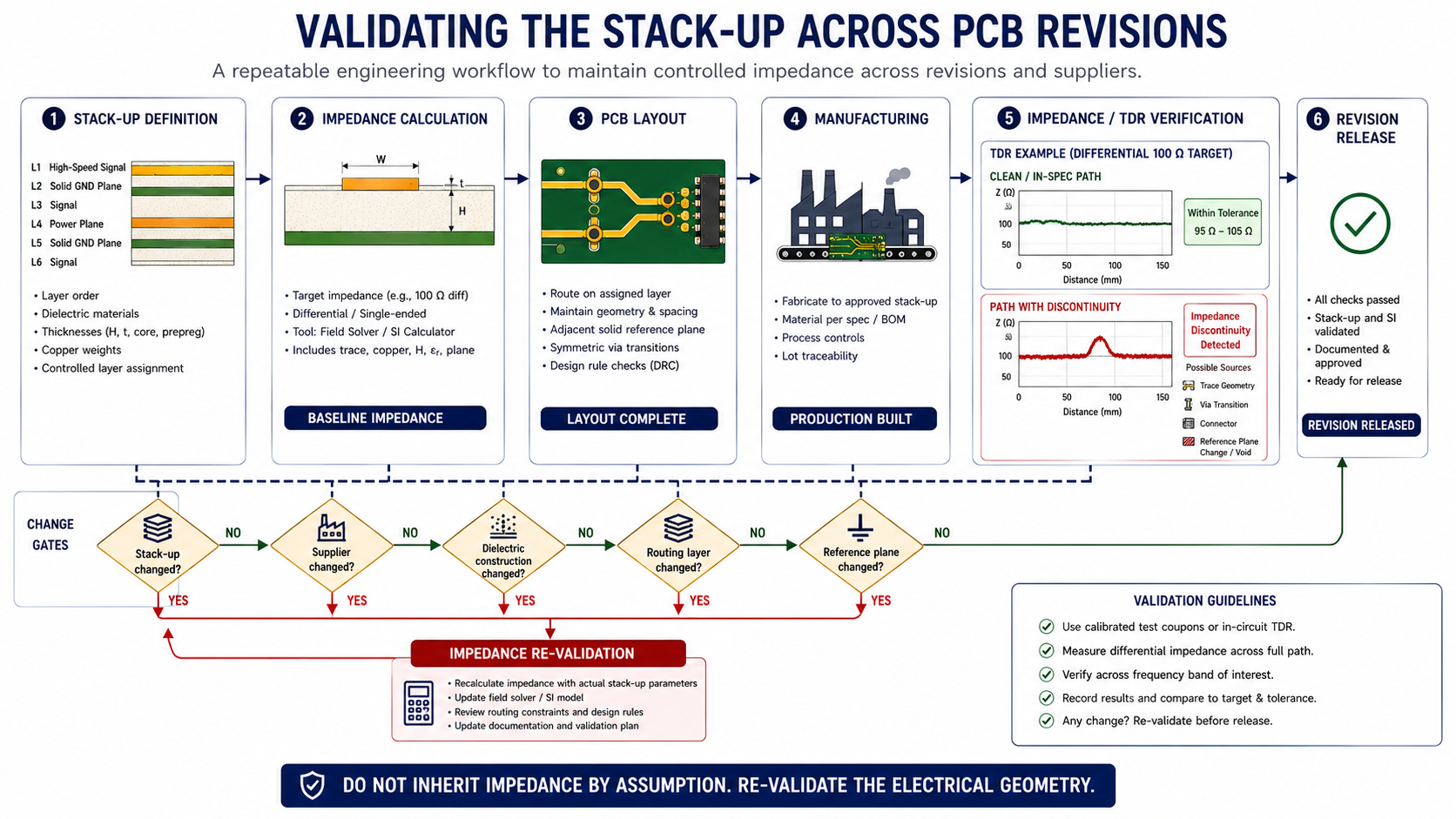
For every meaningful PCB revision, we therefore ask four questions:
Did the stack-up change?
Did the reference plane change?
Did the routing layer or via structure change?
Did the PCB supplier or material construction change?
If any answer is yes, controlled-impedance nets are not automatically considered unchanged.
They are revalidated.
The core principle
A PCB revision should not inherit impedance by assumption.
It should inherit it through a controlled stack-up, defined layer assignments, stable dielectric geometry, explicit manufacturing tolerances, approved supplier constructions, and routing rules that prevent accidental electrical changes.
That is the approach required by a modular architecture such as vBus.
The goal is not to make every PCB identical.
The goal is to make every electrically important decision predictable across boards, suppliers, and revisions.
When that discipline is in place, a new vBus Communication SoM or CPU SoM can evolve without forcing the team to rediscover signal integrity every time the schematic changes.
The stack-up stops being a fabrication drawing.
It becomes part of the architecture.