Finding the Perfect Fit: Board Outline Iteration in Constrained Spaces
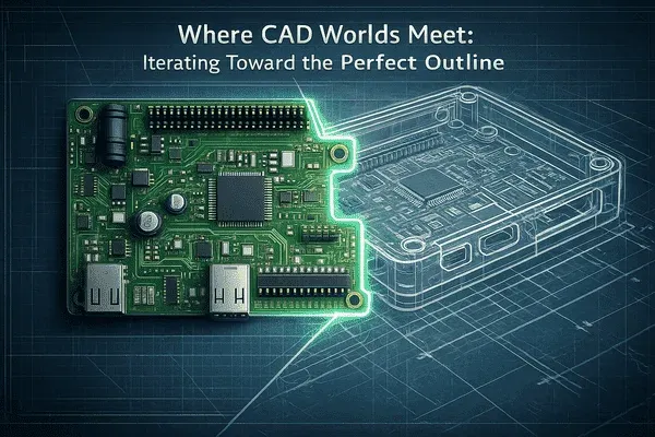
To the untrained eye, it's merely a rectangle, a boundary line. But to us, it's the negotiated truce between electrical ambition and mechanical reality. This outline is not drawn at a whim, it's forged through a rigorous collision of constraints. Component density demands real estate, while enclosure envelopes enforce rigid boundaries. Mounting points anchor the design, while connector placement dictates the flow of the entire harness ecosystem.
For our vBus modular products, this optimization is not just a step, it's the strategy. These modules must inhabit compact enclosures and interface seamlessly through standardized vBus connectors, all while maintaining superior thermal performance. Achieving this balance requires more than just drafting, it demands structured iteration.
Initial constraints: the design envelope
Board outline iteration starts with the enclosure. Maximum PCB size is enclosure internal dimensions minus clearances, typically 2-3mm per side for tolerance stack-up and assembly alignment. Height restrictions come from enclosure internal height minus connector protrusion, typically 10-15mm of available height in consumer products, which determines component packages, QFN over DIP, SMD over through-hole. Wall interference zones from boss posts, internal ribs, and component clearances constrain PCB shape. Early mechanical CAD defines prohibited zones by importing the enclosure 3D model into the PCB tool and overlaying the layout area to identify interference regions.
Mounting requirements matter too. Screw hole positions are dictated by enclosure mounting bosses, typically 3.2mm diameter for M3 screws with a 6-8mm copper-free clearance zone. Mounting hole quantity balances mechanical stability with board area, a minimum of three in a triangular pattern to prevent rotation, four at corners for typical stability, six or more for boards over 100mm to prevent flexing. Standoff height determines bottom-side component clearance and affects thermal contact with the enclosure, typically 3-5mm.
Connector placement adds its own constraints. The vBus connector position is standardized for ecosystem compatibility, edge-mounted with tight alignment tolerance around ±0.2mm for reliable connection. External connectors like USB and power jacks align with enclosure openings at looser tolerances around ±0.5mm. And connector accessibility needs space for mating connector insertion angle, cable bend radius, and strain relief clearance.
Electrical requirements drive area
Mandatory components carry fixed area requirements, a main processor at 10mm by 10mm for a QFN64 up to 14mm by 14mm for an LQFP100, power regulators at roughly 5mm by 5mm each, hundreds of 0402 or 0603 passives. The initial area estimate sums component footprints and adds 40-60% for routing space, traces, vias, clearances, giving a minimum theoretical board area. In one example calculation: major ICs at 200 square mm, power components at 80, passives at 150, connectors at 100, for a component total of 530 square mm, times a 1.5 routing factor, giving an estimated area of 795 square mm, roughly 35mm by 23mm.
Routing density considerations affect achievable density too. Fine-pitch routing at 6 mil trace and space enables tighter packing, while standard 8-10 mil routing needs more area, and power traces at 20-plus mil require dedicated routing channels. Via count, blind or buried versus through, affects both density and cost. And signal integrity for high-speed signals constrains layout, differential pairs need matched length routing that consumes area, clock signals need isolation spacing.
Iteration cycle: refining the outline
The first iteration starts from maximum available area, placing mounting holes at corners and connectors at designated edges, then placing critical components first, followed by high-pin-count components near connectors and passives grouped near associated ICs. Routing critical nets first, then general signals, typically achieves 70-80% completion on the first attempt, identifying congested regions, unreachable pins, and thermal hotspots.
The second iteration integrates mechanical feedback:
- Mounting hole conflicts get resolved by moving holes inboard around enclosure bosses
- Component height issues get resolved by switching to lower-profile connector variants
- Harness routing concerns get resolved by adding keep-out zones for cable bend radius
Board outline adjustments trim corners where components don't reach and extend edges where routing congestion is identified, resulting in an irregular outline optimized for actual component distribution.
The third iteration validates harness integration through 3D routing simulation, modeling connector-to-connector paths, verifying bend radius (typically 6 to 10 times cable diameter), and checking clearance against other harnesses, enclosure features, and heat-generating components. Issues identified at this stage might include a connector too close to a corner needing 12mm clearance where only 8mm is available, solved by shifting the board 4mm away from the corner, or a harness crossing a hot zone above a 5W power regulator, solved by moving the regulator or rerouting the harness.
The fourth iteration optimizes for manufacturing based on DFM feedback from the fabrication partner. Outline complexity matters, straight edges are a standard routing operation while curved edges and internal cutouts add cost, so curves get simplified to straight segments where functionally acceptable. Panel utilization matters too, trimming 2mm from a non-critical edge can increase panel yield by 20-30%. Mounting hole position is adjusted for compatibility with standard test fixture grids, and board edge clearance keeps components 3-5mm from the edge to avoid handling damage.
The fifth iteration validates thermal performance, running FEA with the final board shape and component positions. A typical result: processor temperature at 75°C within limits, power regulator at 82°C acceptable but high, with a 35°C ambient-to-hotspot gradient. Thermal path analysis might reveal the regulator is isolated from the enclosure with poor cooling, solved by extending the board edge 3mm to position it near the enclosure wall with a thermal pad contact point, dropping the regulator temperature to 70°C. Thermal via density under each hot component needs to be adequate, often 30-plus thermal vias.
Final outline: the optimized solution
After five iterations, a typical final board comes in at 48mm by 38mm versus an initial estimate of 35mm by 23mm, a 56% area increase reflecting how often routing complexity gets underestimated initially. The outline is irregular, with corners chamfered to avoid enclosure bosses, and mounting holes positioned per mechanical requirements. All mandatory components are placed, thermal hotspots are managed within limits, and routing completion reaches 100%. Connector positions land within their tolerance windows, vBus at roughly ±0.1mm, USB at roughly ±0.3mm.
Key learnings get captured for next time:
- Initial estimates typically underestimate space needs
- So the routing overhead rule of thumb gets refined from 40-60% to 60-80% for dense designs
- High-speed signals need even more overhead
Early and frequent mechanical review, before routing begins and after routing completion, prevents late changes, and 3D interference checking catches issues 2D review misses. Harness routing drives the outline, cable bend radius is non-negotiable, and simulating harness routing in 3D CAD before finalizing the PCB outline avoids expensive late redesign. And panel efficiency matters, small dimensional changes have large cost impacts, a 2-3mm reduction in a non-critical dimension can increase panel yield 20-30%.
Design process integration
Formal review checkpoints prevent late surprises. Gate 1, the initial outline before layout, involves electrical, mechanical, and manufacturing teams reviewing enclosure CAD, mounting requirements, and connector positions. Gate 2, post-placement before routing, involves electrical and mechanical leads reviewing component placement and a 3D assembly view, checking for mechanical interferences and viable thermal paths. Gate 3, post-routing before release, involves the full cross-functional team reviewing the complete layout, 3D assembly with harnesses, and the DFM report, confirming all routing is complete, all clearances are verified, and manufacturing feedback is addressed.
Documentation standards matter too, the board outline drawing specifies dimensions with tolerances, mounting hole positions and diameters, critical component positions, keep-out zones, and a reference to the enclosure CAD file. Revision control tracks major changes affecting enclosure or mounting separately from minor internal component shifts.
Conclusion: iteration enables excellence
Board outline optimization isn't a single design decision, it's a collaborative, iterative process where electrical needs, mechanical constraints, harness routing realities, and manufacturing efficiency converge into an optimized solution. Each iteration refines the shape, each review catches issues earlier, and each lesson learned informs future designs.
At Hoomanely, we've embraced this structured iteration as an essential discipline. Our vBus modules achieve remarkable density and functionality in compact form factors not through heroic design effort, but through systematic refinement where multiple perspectives shape the final result. The board outline that emerges isn't a compromise, it's an optimized synthesis that delivers electrical performance, mechanical fit, harness accessibility, and manufacturing efficiency simultaneously.