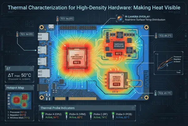
Seeing Heat: Thermal Characterization Strategies for Dense PCB Designs
Our vBus modules represent a feat of extreme integration, condensing high-performance processors, switching power regulators, wireless transceivers, and sensor interfaces into PCBs measuring merely a few square inches. This density introduces a fundamental challenge:
- Heat generation is concentrated
- Thermal gradients are steep
- Component reliability hinges on a precise understanding of exactly how heat flows through the system
We treat thermal characterization not as guesswork, but as a rigorous science of measurement, analysis, and validation that transforms thermal behavior from a mystery into actionable engineering data.
Understanding thermal density
Dense boards create thermal challenges that low-density designs avoid. Heat generation density, total power dissipation divided by board area, runs 0.1-0.5 W/cm² for typical consumer electronics, but 1-3 W/cm² for our high-performance modules, a 5-10x higher thermal density. Component proximity means tight spacing gives limited thermal isolation, adjacent hot components create cumulative heating, and thermal management requires system-level thinking, not just per-component analysis. Limited heatsink real estate means heatsinks compete for PCB area with components, enclosure contact points are limited, and forced airflow is often impractical due to noise, power, or complexity.
Instrumentation: measuring temperature accurately
Thermocouples provide direct, real-time temperature measurement. Type K thermocouples are the standard choice for electronics, covering -200°C to +1350°C at roughly ±2.2°C accuracy. Attachment method is critical for accurate readings, thermally conductive epoxy bonds the thermocouple bead to the component package, placed at the center of the package top surface for ICs or the thermal pad for power components, with wire routing minimizing thermal conduction through the wires themselves.
Strategic sensor placement covers primary hotspots (the main processor, switching regulators, power MOSFETs, wireless power amplifiers), thermal gradient mapping points (PCB corners as coolest zones, mid-board locations, and between closely-spaced hot components for mutual heating analysis), and an ambient reference thermocouple essential for thermal rise calculations. A typical prototype gets instrumented with 8-12 thermocouples covering critical components and gradient mapping points.
Multi-channel data acquisition uses a USB-connected thermocouple interface with 8-16 channel simultaneous sampling at 1-10 Hz to capture thermal transients, logging temperature versus time with timestamp synchronization across all channels, CSV export for post-processing, and real-time alerts when temperatures exceed thresholds. Thermal soak tests run 30-60 minutes to allow the system to reach thermal equilibrium, capturing steady-state temperatures and revealing slow thermal drift or cumulative heating.
Infrared thermal imaging
Thermocouples provide point measurements, thermal cameras reveal spatial distribution. FLIR or Seek Thermal cameras at 320x240 to 640x480 resolution cover -40°C to +550°C at roughly ±2°C or ±2% accuracy, adequate for hotspot identification, at 9-60 Hz frame rate to capture thermal transients.
Imaging procedure matters:
- Horizontal board placement with the camera positioned overhead at a perpendicular viewing angle minimizes emissivity variation effects
- Consistent distance enables calibration and comparison
- A controlled ambient environment minimizes background IR sources
Emissivity compensation is essential since different surfaces radiate IR differently, black soldermask reads accurately at roughly 0.95 emissivity while bare copper reads artificially low at roughly 0.07, so uniform black paint or tape gets applied to metal surfaces, or known-emissivity reference points get used for calibration.
Thermal image capture happens at initial power-on to catch the transient, at steady-state after 30-plus minutes at max load, and during thermal cycling load transitions. The analysis reveals absolute hotspots, thermal gradients, unexpected heat sources, and thermal coupling patterns between components. Before-and-after comparative thermal analysis, baseline capture, implement a fix like thermal vias or a heatsink, re-capture under the same conditions, gives quantifiable improvement statements like "10°C reduction in processor temperature after adding a thermal via array."
Hotspot identification and root cause analysis
Each component has a maximum junction temperature, 85-100°C typical for consumer-grade ICs, 125°C for industrial-grade, 150°C rated for automotive-grade. The design target maintains junction temperature at least 20°C below that maximum, accounting for worst-case ambient (40°C indoor typical), providing a reliability margin, and accommodating measurement uncertainty. For example, a processor rated for 85°C junction temperature gets a target max case temperature of 65°C, a 25°C thermal rise at 40°C ambient, providing 20°C of margin.
Systematic hotspot diagnosis starts with power dissipation verification, measuring actual current consumption against datasheet typical and calculating power to check for unexpected load, incorrect configuration, or component defect. Thermal resistance analysis compares measured thermal rise divided by measured power dissipation against the expected thermal resistance from the datasheet or calculated PCB thermal resistance, a high result indicating inadequate heat spreading or transfer. A thermal path audit checks component-to-copper pad area and via presence, copper-to-internal-plane via count, PCB-to-ambient surface area and airflow, and PCB-to-enclosure thermal interface material and contact pressure.
A worked diagnosis example: a switching regulator measuring 85°C against a 70°C target, with power dissipation measured at 2.5W against a 2.0W datasheet typical. Investigation reveals the input voltage running higher than the datasheet test conditions. Thermal resistance works out to 18°C/W against a datasheet θ_JA of 35°C/W with minimal copper, but the conclusion is inadequate copper area under the device, insufficient thermal spreading.
Thermal fixes: targeted solutions
Thermal via arrays, plated through-holes under the component thermal pad, typically 0.3mm diameter at 0.5-1mm pitch, 20-40 vias for typical QFN or power packages, deliver a 40-60% reduction in thermal resistance, provided they connect to internal ground or power planes for heat spreading. Copper pour expansion, ground plane flooding, wide power traces doubling as heat spreaders, and stitched top-to-bottom copper, delivers a 20-30% temperature reduction for moderately hot components.
Surface-mount heatsinks, aluminum or copper extruded profiles attached with thermally conductive adhesive or tape, increase effective surface area by 10-30x, enhancing natural convection cooling. Sizing is based on component power dissipation, target temperature reduction, and available board space, for example a 2W component targeting a 20°C reduction needs a heatsink rated at 10°C/W or better, typically delivering 30-50°C temperature reduction.
Thermal pads to the enclosure transfer heat from PCB to metal enclosure, positioned between the hottest component and the enclosure inner surface, delivering a 15-25% reduction when the thermal path is established. Enclosure material selection favors metal over plastic, aluminum at roughly 205 W/mK, steel at roughly 50 W/mK, versus plastic at roughly 0.2 W/mK, metal enclosures dissipate heat while plastic insulates.
Component-level optimization includes power supply efficiency (higher efficiency buck converters above 90% typical generate less heat), component derating (power MOSFETs rated for 2x expected current have lower on-resistance, regulators run below absolute max current), and layout optimization (separating hot components to prevent mutual heating, positioning them near board edges for better dissipation).
Validation testing protocol
Maximum load testing operates the system at worst-case power dissipation, all peripherals active, maximum processing load, continuous wireless transmission if applicable, for 60-plus minutes. Elevated ambient testing runs the same load test in a temperature chamber set to the max rated ambient, typically 40-50°C for consumer products, validating junction temperatures stay within limits. Thermal cycling repeats power-on, thermal equilibrium, power-off, cool-down 10-20 times, validating solder joint integrity against thermal expansion and contraction stress and confirming no thermal runaway or cumulative heating issues.
Pass and fail criteria require all components stay below their absolute maximum junction temperature with a 20°C design margin, thermal gradient across the board stays under 30°C (excessive gradient indicates poor heat spreading), and temperatures stabilize within the test duration with no continuous climb.
Documentation and knowledge transfer
Comprehensive thermal test reports capture test conditions, instrumentation setup, measured data, analysis, and conclusions. Annotated thermal images show peak temperature locations, values, hot zones, and reference scale. Lessons learned feed into design standards, minimum thermal via counts, preferred heatsink part numbers, enclosure thermal interface strategies, and component placement rules, all documented for new engineers to learn from characterized designs.
Conclusion: thermal excellence through measurement
Thermal characterization transforms thermal design from guesswork into engineering discipline. By systematically instrumenting prototypes with thermocouples, capturing spatial thermal distributions with infrared cameras, identifying hotspots through analysis, and implementing targeted fixes validated through comparative testing, we ensure every vBus module operates reliably within its thermal envelope.
The investment in characterization pays dividends throughout the product lifecycle:
- Early hotspot identification enables design corrections before volume production
- Validated thermal margins ensure field reliability
- Documented thermal behavior informs future designs
As our modules push density boundaries and power envelopes expand, thermal characterization remains essential infrastructure, making heat visible, making behavior predictable, and making reliability achievable through systematic validation.