Signal Integrity Across Mixed Boards: Engineering Predictability Into vBus PCBs
In the world of hardware development, "prototype" is often synonymous with "experimental." It implies a level of instability that's acceptable for a proof-of-concept but disastrous for a product. In the vBus ecosystem, where CPU SoMs, Power SoMs, Communication modules, and industrial peripherals must coexist in compact enclosures, we cannot afford the luxury of experimental instability.
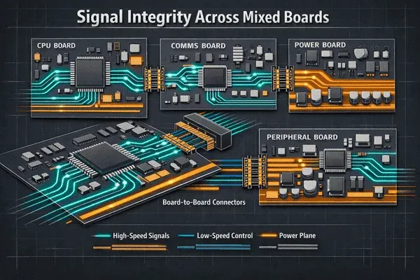
Signal integrity is rarely lost at a single trace or a specific via. In modular systems, it degrades at the boundaries. It fails at the transition between the high-current power domain and the logic domain, it collapses at the board-to-board connector, it unravels when high-speed edge rates encounter the uncontrolled impedance of a generic pin header. For the vBus architecture, signal integrity is not merely a routing concern, it's a system-level discipline.
The physics of the substrate: stackup and materials
The foundation of any signal integrity strategy is the board itself. Before a single component is placed, the stackup dictates the behavior of electromagnetic fields. Standard FR-4 is a cost-effective default, but it's chemically inconsistent. For interfaces like USB 3.0, PCIe, or Gigabit Ethernet running across vBus modules, variations in dielectric constant and dissipation factor can act as a low-pass filter, attenuating high-frequency content and closing the signal eye.
We must account for the fiber weave effect. Standard PCB glass cloth has gaps between the glass bundles. If a high-speed differential pair runs parallel to the weave, one leg might travel over glass while the other travels over resin, creating a propagation delay mismatch that converts differential mode signal into common-mode noise. To mitigate this, we employ zigzag routing or specify spread-glass prepregs to homogenize the substrate environment.
Every high-speed signal in a vBus design requires an uninterrupted reference plane directly adjacent to its signal layer, non-negotiable. We design stackups to minimize the distance between the signal and the reference, which confines fields tightly to reduce crosstalk and allows us to achieve controlled differential impedance with manageable trace widths. The preference is always ground-signal-ground stackups where the reference potential is identical to the shielding potential.
The grounding philosophy: partitioning over splitting
One of the most dangerous myths in mixed-signal design is physically cutting the copper between analogue ground and digital ground to keep them separate. In the vBus architecture, we view physical ground splits as a major hazard.
Current always flows in a loop. At low frequencies, return current follows the path of least resistance, usually the shortest geometric line. At high frequencies, return current follows the path of least inductance, directly underneath the signal conductor. If we physically split a ground plane and route a trace across that void, the return current cannot flow underneath the trace, it's forced to travel around the split to find a bridge, creating a massive current loop area that radiates EMI and absorbs external noise, effectively turning our PCB into a slot antenna.
Instead of cutting copper, vBus boards use component partitioning. We place noisy circuits like buck converters and motor drivers on one side of the board, sensitive analogue circuits like ADCs and sensors on the other, and maintain a single, unified, solid ground plane underneath both. Because high-frequency currents stick tightly to the copper directly under their signal traces, the noise from the buck converter effectively stays in the "noisy" zone without needing a physical cut. If a split is absolutely necessary for isolation standards, we use optocouplers or transformers to bridge the gap, no copper trace ever crosses a void.
Board-to-board connectors as transmission lines
In modular systems like vBus, the board-to-board connector is traditionally the weakest link for signal integrity. We don't assign connector pins based on the convenience of routing, we assign them based on signal return requirements. For every high-speed single-ended signal, there must be at least one adjacent ground pin. For differential pairs, we surround the pair with ground on both sides. This pinout mimics the coaxial structure of PCB routing as it travels vertically through the connector, minimizing the inductive loop through the interconnect.
Even with perfect pinouts, the physical pads of a connector add parasitic capacitance. On vBus boards, we often employ voiding on the reference layers directly beneath the connector signal pads, removing the ground copper on the layer directly under the connector pad to increase the distance to the reference and reduce excess capacitance. This technique helps maintain the impedance target right up to the metal contact, preventing signal reflections.
Routing strategy: managing energy fields
We view routing not as "connecting dots" but as guiding electromagnetic waves. In the dense real estate of a vBus module, traces are often forced close together, inviting crosstalk, the capacitive and inductive coupling of energy from an aggressor trace to a victim trace. To mitigate this, we adhere to the 3W rule: the distance between the centers of two aggressive high-speed traces should be at least three times the width of the traces, reducing coupling flux by roughly 70%. For critical clock lines or extremely sensitive analogue inputs, we may use a guard trace, though guard traces are a double-edged sword, if not stitched to the main ground plane at regular intervals, they can become resonant antennas. We prioritize spacing over guard traces unless absolutely necessary.
For differential signals, symmetry is more important than absolute length. It's not enough for the positive and negative traces to be the same total length, they must be phase-matched at every turn. If the P trace travels longer than the N trace through a bend, the signal briefly becomes common-mode noise, so we use small "phase bumps" immediately near the mismatch to correct this locally. We also ensure the fiber weave effect doesn't de-skew our perfectly matched lines.
Power integrity as a signal integrity multiplier
You cannot have clean signals without a clean reference. When a digital IC switches, it draws a sudden gulp of current. If the power distribution network has high impedance, this current demand causes the voltage rail to dip, and that ripple propagates through the driver and appears as jitter on the output signal.
vBus designs treat the power rail as a frequency-dependent impedance profile:
- The voltage regulator module handles low-frequency current demands
- Bulk capacitors handle the mid-range
- Ceramic decoupling handles high frequencies
- Plane capacitance
- Formed by the power and ground planes sandwiching the dielectric
- Handles ultra-high frequencies
We select capacitors not just for their bulk value, but for their equivalent series resistance and equivalent series inductance, placing the smallest, lowest-inductance capacitors closest to the IC power pins to provide immediate energy for edge transitions. This ensures the reference voltage remains stable even during aggressive switching, preserving the vertical opening of the signal eye diagram.
Validation: simulation and measurement
The "behavior" of a prototype is the final exam, but we don't wait for the hardware to arrive to know the answer. Before a route is finalized, we use IBIS models provided by silicon vendors to simulate critical nets, checking whether we need series termination resistors to dampen ringing, what the maximum allowable trace length is before signal degradation occurs, and whether the drive strength of the output buffer is sufficient for the capacitive load.
Once the board is routed, we use 2.5D or 3D field solvers to analyze coupling, looking for accidental impedance changes, like a trace passing over a void in the ground plane that was missed by the human eye. When the vBus prototype arrives, we validate the simulation against reality using time domain reflectometry, sending a pulse down the line and watching the reflections, literally "seeing" the connector, the via, and the trace segment on the oscilloscope screen, identifying exactly where impedance mismatches occur.
Conclusion: signal integrity as confidence
Signal integrity is not a dark art, it's physics. It's the rigorous application of Maxwell's equations to copper and fibreglass. In the vBus ecosystem, we don't view SI as a checklist item to be addressed at the end of the design cycle. It's an architectural constraint that informs every decision, from the selection of the laminate material to the assignment of a connector pin, to the placement of a decoupling capacitor.
By treating signal integrity as a system property, we ensure our prototypes function not just as "proofs of concept," but as "proofs of manufacturability." We eliminate the ghosts in the machine, the random resets, the data corruption, the inexplicable EMI failures, before they ever manifest. When signal integrity is engineered in, through robust stackups, disciplined return paths, and proactive power integrity, prototypes stop being experiments. They become reliable, predictable, production-ready assets.