Designing Dual-Camera Support on a Single CSI-2 Port with Minimal GPIOs
The problem
We needed two cameras on a TI AM62A7-Q1, and the SoC gives us exactly one MIPI CSI-2 receiver. It is a 4-lane port, and the cameras we picked are IMX708 modules in the Raspberry Pi Camera Module 3 class, each running 2 data lanes.
The first idea everyone has is simple arithmetic. Two lanes plus two lanes is four lanes, so wire camera A to lanes 0 and 1, camera B to lanes 2 and 3, and call it done.
It does not work. The AM62A has one D-PHY with one clock lane, and every data lane on that PHY is timed by that single clock and belongs to a single CSI-2 link. Each IMX708 drives its own clock lane and its own independent packet stream, and the PHY has no mode that splits it into two 2-lane receivers.
There is a second, quieter problem. Both IMX708 modules sit at the same fixed I2C address, 0x1A. Even if the data path were solved, the control path would collide.
So the real question became: what is the least hardware, firmware and pin cost to get two of these cameras working on one port?
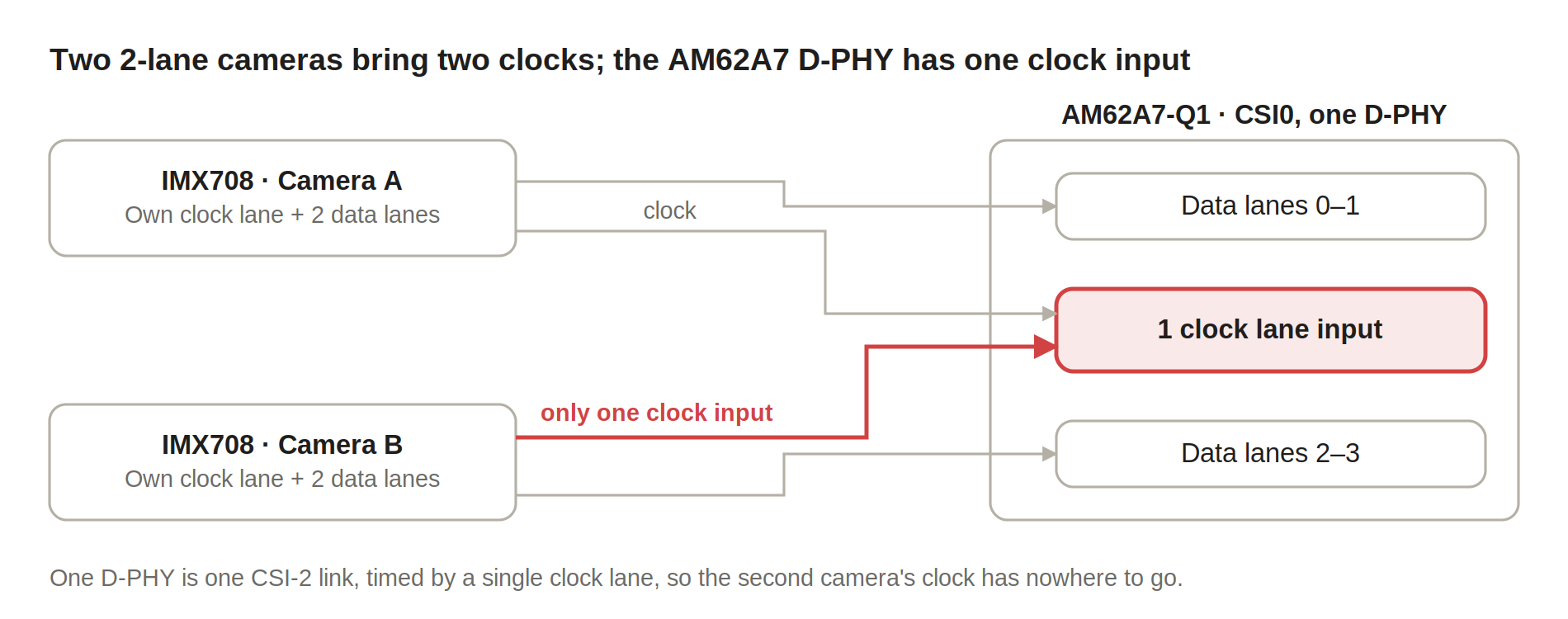
The lane count adds up, but the clock count does not: each IMX708 needs its own clock lane, and the receiver has only one.
Options we evaluated
Every proven way to put multiple cameras on one CSI-2 port does the same thing underneath. Something merges the streams before the SoC and tags each one with a CSI-2 virtual channel, and the AM62A receiver splits them back out. The options differ in what that something costs you.
FPD-Link III/IV deserializers such as the DS90UB954-Q1 (two inputs) or DS90UB960-Q1 (four inputs) are TI's reference multi-camera path on this SoC. They give simultaneous capture, frame sync and mainline Linux drivers. But every camera needs its own serializer, and for cameras sitting on the same board that is a lot of silicon to move data a few centimetres.
GMSL2 deserializers like the MAX9296A or MAX96712 do the same job. Driver support on TI's SDK is less turnkey, so we would have been porting and debugging that ourselves.
An FPGA aggregator, for example a Lattice CrossLink-NX running a CSI-2 virtual channel merge IP, avoids SerDes entirely. It still adds an FPGA, its power rails, a bitstream to maintain and a custom V4L2 driver.
A passive MIPI switch is the minimal option. It physically connects one camera at a time to the port, with one select line and no protocol logic at all.
A USB UVC camera as the second input was the fallback. It bypasses the SoC's ISP, so it was never a real candidate.
Our product did not need both cameras streaming at the same time, so we went with the passive switch. The trade-off is real and worth stating plainly: only one camera streams at a time, and switching takes roughly 100 to 300 ms. That time is spent stopping the stream, flipping the switch, reprogramming the sensor and restarting.
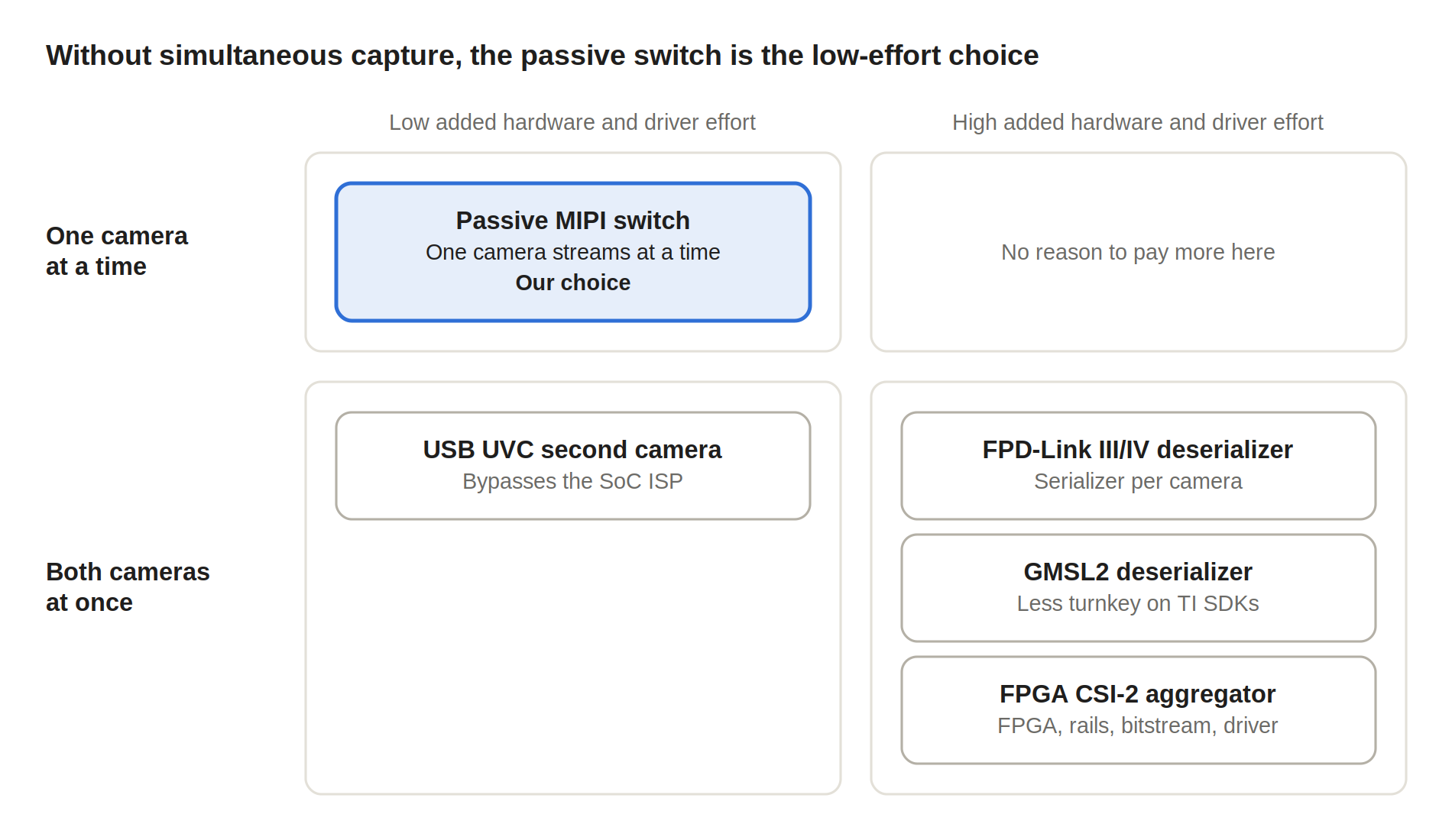
Every option that streams both cameras at once either bypasses the ISP or adds significant hardware and driver work.
Choosing the MIPI switch: TMUX646 vs TS3DV642-Q1
We shortlisted two TI parts, the TMUX646 and the TS3DV642-Q1. Both are passive, bidirectional 2:1 high-speed switches, and both have bandwidth far beyond what the IMX708 needs at roughly 900 Mbps per lane.
The TMUX646 is the obvious first pick. It is tiny, a 2.45 mm nFBGA, it switches 5 differential pairs (one clock plus four data lanes), and it runs from a wide supply range.
Two things pushed us away from it. It is rated only to 85 °C ambient with no automotive grade, and it has a 0.4 mm ball pitch with interior balls that need via-in-pad or HDI to escape. On a carrier board that otherwise does not need HDI, that one part would set the fabrication cost.
The TS3DV642-Q1 is AEC-Q100 Grade 2, rated from -40 to 105 °C. It switches 6 differential pairs, comes in a WQFN package that routes, inspects and reworks easily, runs from 3.3 V and accepts 1.8 V-compatible control logic.
We picked the TS3DV642-Q1. The switch sits inside an enclosure next to the SoC, where local temperature runs well above room ambient, and its grade matches the -Q1 SoC it serves. Removing the HDI requirement was a bonus.
The trade-offs are acceptable. The footprint is several times larger, the supply is fixed at 3.3 V, and insertion loss at multi-GHz is a little higher. At our roughly 450 MHz fundamental, that loss does not cost meaningful D-PHY margin.
One tip from this stage: route all four data lanes through the switch even though the IMX708 uses two. The extra traces cost almost nothing, and a 4-lane sensor can drop in later without a board respin.
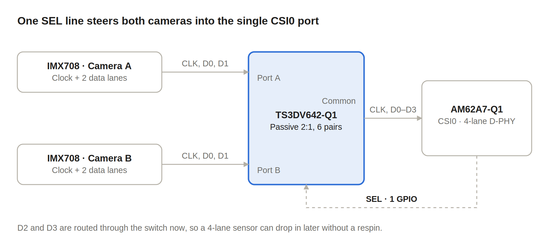
The switch connects one camera's clock and data lanes to CSI0 at a time, chosen by a single GPIO.
Solving the shared I2C address
With the data path settled, both cameras still answered at 0x1A. We looked at four ways out.
Two native AM62A I2C controllers, one per camera, is the cleanest on paper. It costs four SoC pins and assumes the I2C bank voltage matches the modules, or else needs a level translator on each bus.
An I2C address translator such as the LTC4316 can remap one camera to a new address on a shared bus. It works, but it is a niche part for a problem a simpler switch solves.
Routing SDA and SCL through the spare channels of the MIPI switch looked free. The TS3DV642-Q1 is passive and passes DC, so electrically it works, and the I2C lines would follow SEL automatically.
The catch was software. Linux cannot register two devices at 0x1A on the same I2C adapter. The shared select line would have to drive both a video mux and an I2C mux through the mux framework, an unusual arrangement we did not want to debug in the field.
We chose the TCA9543A, a 2-channel I2C switch. The SoC sees one bus, the TCA9543A presents two isolated downstream channels, and each IMX708 keeps its 0x1A address on its own channel. The mainstream i2c-mux-pca954x driver handles it, so each camera simply appears on its own child bus.
It also handles a voltage mismatch for free. Pull the upstream side up to the SoC's I/O voltage and each downstream channel to 3.3 V, and the passgate switch translates between them.
One rule we kept even with only one camera powered at a time: never put both modules directly on one bus. An unpowered module's level shifter or ESD structures can load or clamp SDA and SCL, and the TCA9543A disconnects the idle channel completely.
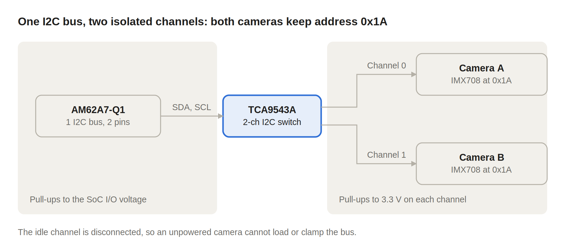
The TCA9543A sits across the two voltage domains, so the same part fixes the address clash and the level mismatch.
Pin budget, power and control
The whole dual-camera setup uses 3 required GPIOs, 2 I2C pins and the dedicated CSI balls. We counted every pin before choosing parts, because only true GPIOs compete with the rest of the system.
Resource | Pins | Notes |
|---|---|---|
CSI0 clock and data lanes | 6, or 10 with 4-lane routing | Dedicated CSI balls, not GPIOs |
I2C to the TCA9543A | 2 | One bus for both cameras |
Switch SEL | 1 GPIO | Required |
Camera A power enable | 1 GPIO | Required |
Camera B power enable | 1 GPIO | Required |
Switch power-down | 1 GPIO, optional | Can be tied to the enabled level |
TCA9543A reset | 1 GPIO, optional | Can be pulled high |
The SoC does not need to provide a sensor clock. The Pi-class camera modules carry their own 24 MHz oscillator, so there is no MCLK line to route.
We could have derived both camera enables from SEL through an inverter and saved two more GPIOs. We chose not to. Separate enables let us power both cameras down, and power-cycle a hung sensor without touching the switch, which matters for units in the field.
There are four voltage domains to keep straight. The AM62A CSI analog rail is 1.8 V, the switch runs at 3.3 V, the camera connector supplies 3.3 V with 3.3 V I2C and enable logic, and the SoC's I2C bank may be 1.8 V, which the TCA9543A pull-ups bridge. Check exact rail values and camera current draw per the datasheets.
Our bring-up order is fixed. Rails come up first, then SEL is set, then the selected camera is enabled. We wait for the module regulators, select the matching TCA9543A channel, probe the sensor, and start streaming. The unselected camera stays powered off.
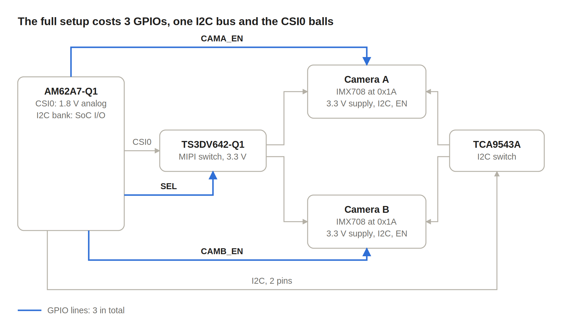
Only the three highlighted lines are true GPIOs; the lanes and the I2C bus use dedicated or pin-muxed peripheral pins.
Layout guidelines
A passive switch is only as good as the traces around it. The rules we followed are standard D-PHY practice, applied with the switch in mind.
- Route 100 Ω differential pairs over a continuous ground plane, with tight intra-pair matching and lane-to-clock matching per the AM62A hardware design guide.
- Avoid stubs, keep vias to a minimum, use two 45° bends instead of a 90° turn, and keep pairs away from switching regulators, crystals and mounting holes.
- Place the switch close to the SoC or SOM so the shared trunk is short, and keep the two camera branches similar in length so both cameras see the same channel.
- Terminate or tie off unused switch channels exactly as the TS3DV642-Q1 datasheet recommends, rather than carrying over another part's advice.
- Put low-capacitance ESD protection at the FPC connectors if they are reachable by users or assembly staff.
At around 900 Mbps per lane, none of this is exotic. The point is that the switch adds a discontinuity in every lane, so the rest of the channel should not add more.
Software side
The hardware choices were made so the Linux side stays boring. Every piece maps to an existing, mainstream driver.
On the I2C side, the TCA9543A is described with i2c-mux-pca954x. It creates two child buses, and each one carries an imx708 node at address 0x1A, so the kernel never sees a conflict.
On the CSI side, the SEL GPIO becomes a gpio-mux controller consumed by the Linux video-mux driver. The video-mux has two sink endpoints, one per IMX708, and one source endpoint to CSI0 with data-lanes set to lanes 1 and 2.
Switching cameras is then a media-ctl link change. Stop the stream, change the active link on the video-mux, and start streaming again. That sequence is where the 100 to 300 ms switch time comes from.
Three practical gaps are worth knowing before you start:
- The IMX708 driver, and the VCM driver needed for autofocus, live in the Raspberry Pi kernel tree, not in TI's SDK, so they have to be ported.
- TI does not ship DCC tuning files for the IMX708. Without tuning, the VPAC ISP output will not look good, so plan for a tuning pass with TI's tools.
- The IMX708 has no usable hardware frame sync on standard modules. Treat the two cameras as unsynchronized, which is fine for a design that only streams one at a time.
Takeaways
If you do not need simultaneous capture, a passive MIPI switch plus an I2C switch is the lowest-complexity way to get two cameras onto a single-port SoC. On the AM62A7-Q1 it cost us two small chips, one I2C bus and three GPIOs.
If you do need both cameras streaming at once, there is no shortcut. Step up to a CSI-2 virtual channel aggregator in an FPGA, or to a SerDes deserializer, and budget for the extra parts, pins and driver work.
Pick the switch for your thermal and qualification needs, not just its bandwidth. Almost any modern MIPI switch has the bandwidth; far fewer have the grade and package that suit your enclosure and your board stack.
And count pins before you pick parts. Separating dedicated CSI balls and pin-muxed I2C from true GPIOs showed us where savings actually mattered, and where saving one more pin would have cost us field reliability.