Designing for EMI from Day Zero — How We Engineer Certifiable Hardware at Hoomanely
In modern connected hardware, especially the kind we build at Hoomanely, where a single board includes radios, sensors, power switching, ADCs, cameras, and compute, one silent enemy keeps showing up in product timelines: electromagnetic interference. But here's the twist: EMI is predictable. When we design a PCB with EMI principles from revision zero, we remove uncertainty from certification, reduce debug time, and eliminate the risk of costly re-spins. At Hoomanely, we don't fix EMI. We engineer products so EMI never becomes a problem.
What EMI actually means in hardware product design
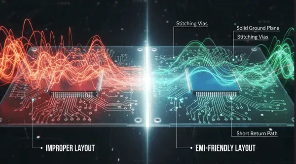
Every trace that carries a fast signal radiates electromagnetic energy. Every return path that detours around a gap becomes a loop antenna. Every switching regulator, WiFi module, and high-speed bus introduces broadband noise. If not controlled, these tiny radiators interact with your own sensors as intra-device interference, nearby electronics as inter-device interference, and regulatory thresholds for FCC, CE, and IC compliance. Rather than chasing noise after the first certification failure, we embed electromagnetic behavior into our routing rules from the beginning. At Hoomanely, EMI is treated as a design parameter, not a debugging phase.
Four EMI principles applied on every board
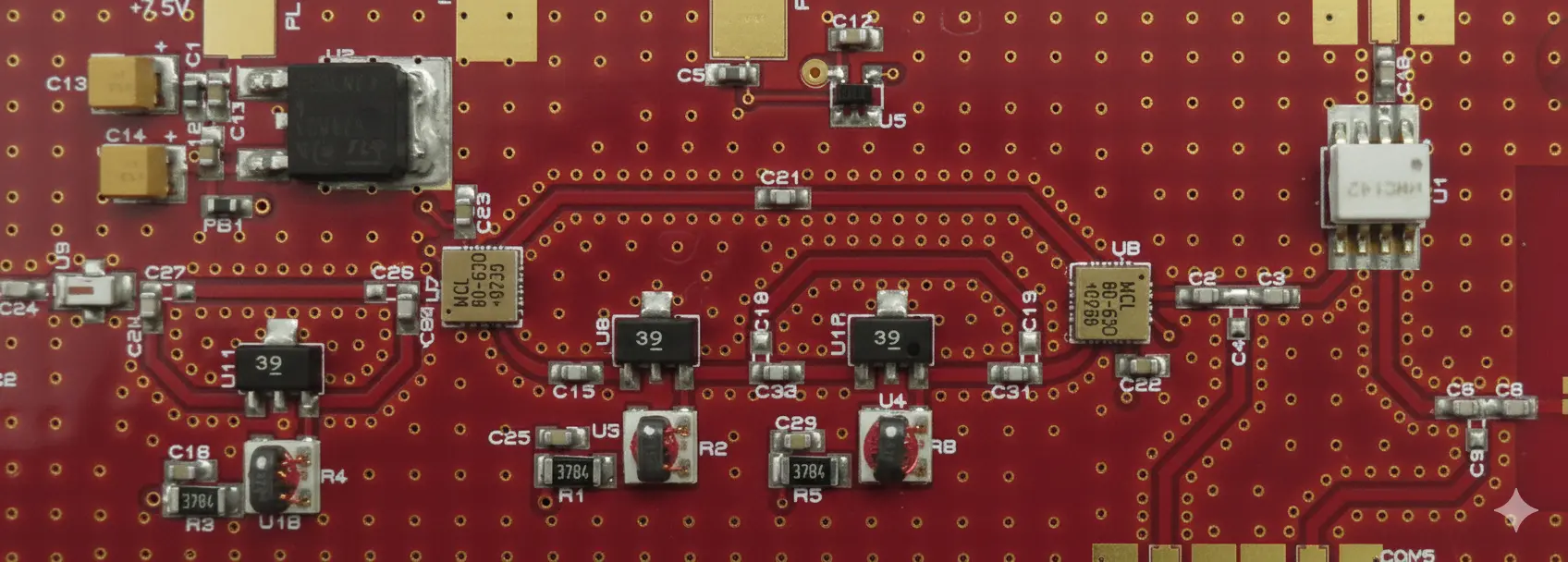
Stitching vias create controlled electromagnetic boundaries. We place them extensively along board edges, forming a ground cage, surrounding EMI-prone circuits like switching supplies and radios, and near transitions between signal layers to give return currents a direct path. Think of stitching vias as walls that contain high-frequency currents. By spacing them roughly every 10-20mm, about one-sixth wavelength at digital harmonics, we reduce radiated emissions significantly, consistently improving margins without requiring metal shielding cans, reducing BOM cost and simplifying mechanical assembly.
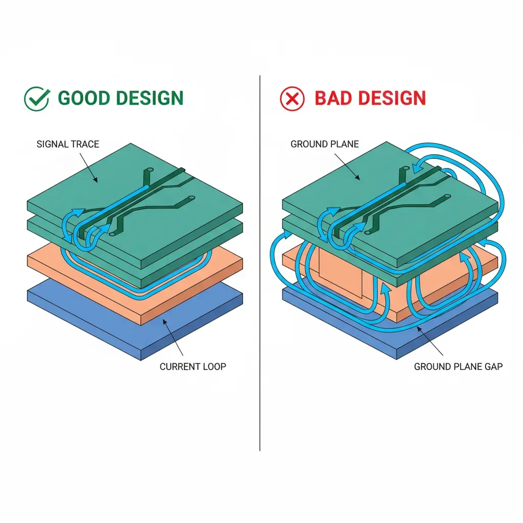
Solid ground planes are the silent hero of signal integrity and EMI. A PCB with a continuous ground plane behaves like a controlled RF environment, giving a low-impedance return path and minimal loop area, preventing unpredictable return current detours from segmentation, and acting as a shield containing electromagnetic fields internally.
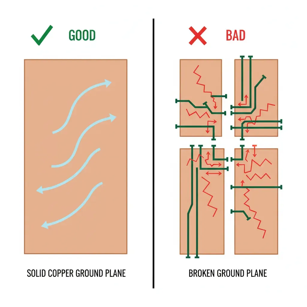
Return path engineering controls the loop area. A signal leaving an IC must return to the source, always. At low frequencies, current follows the path of lowest resistance. At high frequencies, current follows the path of lowest inductance, directly under the signal trace. So we design for controlled return paths, high-speed traces always routed over an uninterrupted ground plane, no ground gaps under USB, Ethernet, SPI, or clock lines, and differential pairs tightly coupled to minimize loop area. EMI is proportional to loop area, reduce the loop and you reduce EMI. This design discipline ensures USB, PCIe, and WiFi coexist without injecting noise into sensor analog paths.
Decoupling network strategy eliminates noise at its source. Instead of just placing capacitors near the pins, we treat decoupling as localized energy absorption:
- Caps placed within 3-5mm of IC pins
- Dedicated vias to power plane and ground with no shared vias
- A multi-value capacitor stack combining bulk
- Mid-frequency
- High-frequency capacitance
This ensures switching currents never travel far enough to radiate. Good decoupling is the difference between a stable system and a noisy board.

Beyond EMI: the engineering advantages we consistently see
When EMI is addressed from day zero, faster certification means no redesign cycles and faster time to market. Better radio performance comes from a cleaner RF environment giving higher sensitivity. Reliable sensor readings mean no random noise-induced glitches. Reduced cost means no shielding cans and fewer filter components. Teams that only aim to pass EMI tests stop at compliance. We design for predictability, reliability, and scale.
The EMI checklist before sending a board to fabrication
Before a layout is marked complete, it must pass a gate confirming a solid, uninterrupted ground plane, stitching vias every 10-20mm around edges, via fences around switching regulators and radios, high-speed signals routed directly over the ground plane, no signal crossing that breaks ground return paths, decoupling caps within 3-5mm of IC power pins, and differential pairs that are length- and impedance-matched.
Final thoughts
EMI-first design is not about avoiding failure, it's about engineering confidence. PCB layout stops being guesswork and becomes a controlled, high-repeatability process. Radios behave predictably, sensors stay clean, certification becomes a formality. At Hoomanely, EMI awareness is not a patch, it's baked into our engineering culture.