Designing vBus: A Universal Bus Architecture for Modular Embedded Systems
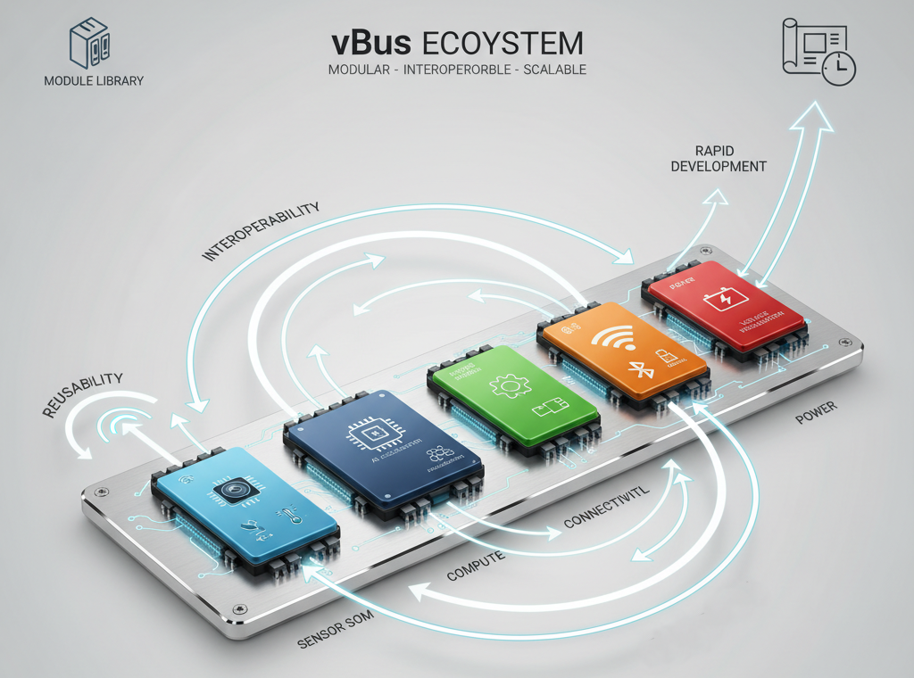
In embedded systems development, one of the most persistent challenges is creating hardware that's both flexible and standardized. At Hoomanely, we've tackled this challenge head-on by developing vBus, a universal communication bus architecture that serves as the backbone for all our product lines. Think of it as the USB of our ecosystem, but purpose-built for System-on-Module interconnectivity.
The concept is elegantly simple: every functional module communicates with the rest of the system through a standardized interface. Whether it's a sensor module, a processing unit, or a power management board, they all speak the same language through vBus. As with most engineering challenges, though, the devil is in the details.
Connector selection: the goldilocks problem
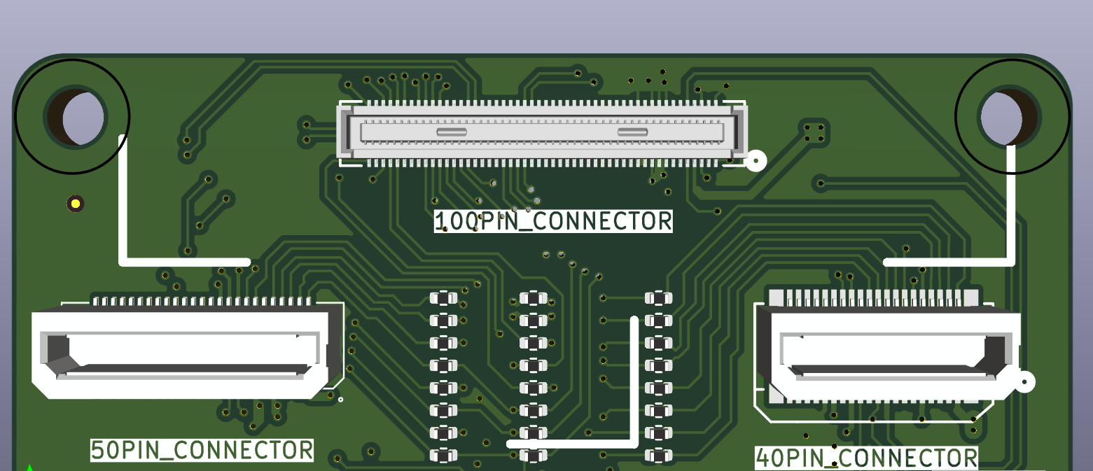
The first challenge seems straightforward: choose a connector. But when SOMs range from tiny sensor boards measuring a few square centimeters to larger processing modules with extensive I/O, finding a connector that works for everyone becomes a complex optimization problem. A small sensor SOM might have limited PCB real estate where a large, high-pin-count connector would dominate the board, while a minimal connector on a feature-rich module would create a bottleneck forcing daisy-chaining or custom breakout boards.
Our approach defines a family of connectors rather than a single solution, think S, M, L, and XL variants, establishing a hierarchical pinout where the most critical signals occupy consistent positions across all connector sizes, selecting connector types with high pin density while maintaining reliable manufacturability, and considering both vertical and horizontal mounting for different form factors. The key insight is that true modularity doesn't mean identical, it means compatible. Our connector strategy allows designers to choose the right tool for the job while maintaining interoperability through careful pinout planning.
Communication interface diversity: speaking multiple dialects
Modern SOMs aren't one-size-fits-all, and neither are their communication requirements. A high-speed camera module might need PCIe or high-speed LVDS for gigabit video streaming, while a simple temperature sensor might only need I2C at a few hundred kilohertz, and an actuator control module might require high-precision PWM with strict timing. The challenge is threefold, speed diversity between multi-gigabit differential pairs and simple GPIO, protocol variety across UART, SPI, I2C, CAN, USB, Ethernet, MIPI-CSI, and LVDS, and signal integrity for high-speed data while keeping connectors and traces cost-effective.
Our solution allocates dedicated lanes for high-speed differential pairs with controlled impedance routing guidelines, reserves a pool of configurable pins serving multiple protocols through software configuration, implements a signal classification system (power, high-speed data, low-speed control, analog) guiding both pin assignment and PCB layout, and includes sideband communication channels like I2C letting modules identify themselves and negotiate capabilities. This allows a designer to build a minimal sensor node using just low-speed pins while another engineer develops a vision module leveraging high-speed lanes, both using the same fundamental vBus architecture.

Power distribution: more than just voltage rails
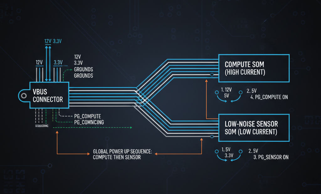
Power delivery in a modular system is remarkably complex. A processing SOM might need 5V at 3A, 3.3V at 500mA, and 1.8V at 200mA. A motor control module might require 12V at 5A with back-EMF protection. A sensor board might run on 3.3V at just 50mA but need ultra-low noise for analog measurements. The challenges include current capacity (connector pins have maximum ratings, running 5A through a pin designed for 1A creates heating and voltage drop), pin allocation (more power pins means fewer signal pins), voltage selection (raw voltages for each SOM to regulate, or multiple regulated rails), and ground integrity competing for connector real estate.
Our power strategy dedicates multiple parallel pins for high-current rails, effectively multiplying current capacity, provides a mix of raw battery voltage for power-hungry components and regulated common voltages for ease of use, implements a separate ground pin allocation ensuring low-impedance return paths, includes power-good and enable signals for sequencing, and documents maximum current budgets per rail with design guidelines for SOM power consumption. The goal is power distribution robust enough for demanding applications while remaining simple for basic modules.
Debug and boot infrastructure: the hidden complexity
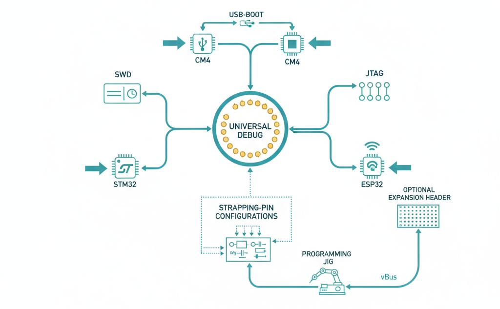
Every microcontroller and processor has its own requirements for programming, debugging, and boot configuration. An STM32 uses SWD with two pins, an ESP32 needs specific strapping pins during boot, a compute module requires USB boot modes, an NXP processor might need JTAG. The complications include incompatible debug protocols across architectures, boot mode selection requiring specific pins pulled high or low at power-up, some processors needing dedicated debug connectors while others share pins, and pin count limitations forcing difficult prioritization.
Our approach reserves a debug pin group supporting multiple protocols through careful selection, defines a boot configuration standard using a minimal pin set compatible across architectures, provides optional expansion headers for architecture-specific debugging, includes I2C-based GPIO expanders for remote boot mode configuration, and creates programming jigs accessing the vBus connector directly, eliminating per-module debug headers. This standardization dramatically reduces the learning curve moving between SOM types and enables common tooling across the entire ecosystem.
The bigger picture: why universal interfaces matter
The vBus architecture isn't just an engineering exercise, it's a business and development velocity enabler. Faster development cycles let engineers mix and match modules without redesigning interconnects for each project. Cost optimization comes from standardized connectors and interfaces allowing volume purchasing and reduced SKU proliferation, a single backplane design hosting multiple SOM configurations. Future-proofing means new SOMs automatically integrate with existing carrier boards, protecting our ecosystem investment. Easier testing and validation comes from common interfaces meaning common test fixtures. And customer flexibility lets end-users upgrade or reconfigure systems by swapping modules without hardware redesign.
Conclusion
Designing the vBus architecture has been an exercise in systematic constraint resolution. Each challenge, connector selection, interface diversity, power distribution, debug infrastructure, requires balancing competing requirements while maintaining the core promise of universal modularity. The result is an architecture that doesn't try to be everything to everyone with a single massive connector, but instead provides a flexible framework that scales from simple sensor nodes to complex processing systems. Good standardization isn't about rigidity, it's about creating enough structure to ensure compatibility while leaving room for innovation within that framework.