Inside the vBus Ecosystem: A Deep Dive into Hoomanely's SoM Architecture
We've introduced vBus, our universal communication bus architecture that forms the backbone of Hoomanely's modular ecosystem, and discussed the challenges of creating a standardized interface that could accommodate diverse modules with varying requirements. Now it's time to pull back the curtain on what sits on either end of those vBus connections: the System-on-Modules themselves.
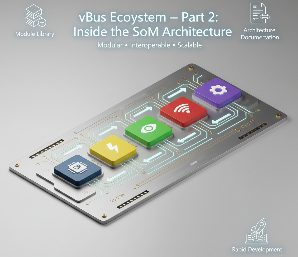
Building a truly modular embedded platform isn't just about creating a clever connector standard. It's about architecting a family of intelligent modules that work in concert, each optimized for its specific role while maintaining seamless interoperability. We've developed four distinct SoM categories, each with its own architectural considerations and pin-out strategies.
The CPU SoM: the orchestral conductor
The CPU SoM is the brain of our ecosystem, the central processing hub coordinating data flow, executing application logic, and managing the entire system. A modern application processor can expose hundreds of potential I/O pins, USB ports, Ethernet controllers, display interfaces, memory buses, GPIO banks. We settled on a 100-pin connector standard after extensive analysis, organized into aggressive pin blocks. The Power Block handles multiple voltage rails with parallel pins for high-current delivery, power-good signals, and enable controls. The High-Speed Communication Block carries carefully impedance-controlled, isolated lanes for simultaneous high-bandwidth connections. The Low-Speed Communication Block carries UART, SPI, I2C, and GPIO connecting to peripheral SoMs, with multiple instances of common protocols, like three independent I2C buses, to prevent bottlenecks. The Programming and Debug Block carries JTAG/SWD, UART console, and boot mode selection. The Special Function Block covers analog inputs, PWM outputs, interrupt lines, and reserved expansion pins.
The real engineering challenge wasn't deciding what to include, it was deciding what to leave out. Every pin is a compromise. We approached this through extensive application analysis, identifying the minimum set of interfaces that 80% of target applications would need directly on the CPU SoM. For the remaining 20%, peripheral SoMs and ecosystem flexibility come in, need industrial RS-485? Add a peripheral SoM handling protocol conversion. This architecture also enables CPU SoM swapping, a project might start with a dual-core Cortex-A7 for basic applications and swap in a quad-core Cortex-A53 or octa-core Cortex-A72 as requirements grow, without redesigning the system, as long as the core pinout remains consistent.
The Power SoM: small but mighty
If the CPU SoM is the brain, the Power SoM is the heart. Don't let its compact 30-pin standard fool you, this module deals with some of the highest electrical stresses in the entire ecosystem. I2R losses are the enemy, push current through a connector pin and resistance causes voltage drop and heat, double the current and you quadruple power dissipation. Our Power SoM delivers potentially 50-100W of total power through a compact connector, if we're providing 5V at 10A that's 50W, and a typical board-to-board pin rated for 3A continuously can't handle that alone.
Our solution is parallel pin allocation, for a 5V/10A rail we use 4-5 pins each carrying 2-2.5A, distributing thermal load and reducing overall resistance, with ground return getting the same treatment. But the Power SoM isn't just a dumb power supply, it's intelligent, using a dedicated I2C or SPI connection to the CPU SoM to report real-time voltage and current per rail, temperature monitoring, fault detection, battery status, and power sequencing health. This bidirectional communication enables sophisticated power management, the CPU SoM can query consumption, dynamically throttle performance to stay within thermal limits, or shut down non-critical peripherals to conserve energy on low battery. Connector selection matters too, we needed high current rating per pin, low contact resistance under 10mOhm, robust mechanical design for repeated mating, good thermal conduction, and a compact footprint despite high pin count.
Peripheral SoMs: the future is modular
This is where the vBus ecosystem truly shines. Peripheral SoMs are our plug-and-play sensor and actuator modules, representing a fundamental shift away from cramming every possible sensor onto a monolithic board. Each Peripheral SoM is built around a 40-pin standard connector and includes an onboard MCU, a crucial decision solving multiple problems at once.
Protocol translation means sensors speak dozens of different languages, I2C, SPI, analog voltage, pulse trains, proprietary protocols. Rather than forcing the CPU SoM to directly support every interface, we embed intelligence in the Peripheral SoM, the onboard MCU reads the sensor natively and translates to a standardized format over vBus. Data preprocessing handles filtering, calibration, unit conversion, and sensor fusion locally, sending only meaningful data, a motion sensor module might perform IMU fusion onboard and send orientation quaternions rather than raw readings. Reduced system complexity means the CPU SoM no longer needs a dozen different sensor drivers, communicating over a few standard protocols while each module manages its own sensor. Hot-swappability means the system can auto-detect and configure new peripherals, plug in a new sensor module and it identifies itself over I2C, downloads calibration data, and starts reporting.
The 40-pin standard breaks down into a Power Block (typically 3.3V and 5V with adequate ground, modest requirements compared to CPU or Power SoMs), a Primary Communication Block (high-speed connection to the CPU SoM, usually SPI or UART plus I2C for configuration), a Secondary Communication Block (analog inputs, interrupt lines, GPIO for indicators), a Programming Block (SWD or UART bootloader for the onboard MCU), and Expansion/Reserved pins for future capabilities. Real-world variants include an Environmental Sensor SoM (temperature, humidity, pressure, air quality reported as clean data), a Vision SoM (camera with onboard image processing, even edge ML inference), an Industrial I/O SoM (isolated digital I/O and analog conditioning), and a Motor Control SoM (high-current drivers with encoder feedback and local position control).
The Communication SoM: gateway to the world
The Communication SoM bridges the local vBus ecosystem and the outside world, whether cloud, smartphone, or mesh network. Modern IoT applications generate substantial data, a vision system might produce megabytes per second, a multi-sensor industrial monitor could stream hundreds of telemetry channels, all needing wireless transmission with real-time requirements. This is why the Communication SoM uses a 50-pin connector standard emphasizing high-speed interfaces, dedicated lanes for USB 2.0/3.0, SDIO, or even PCIe for high-performance wireless modules, capable of hundreds of megabits per second.
The architecture accommodates different wireless technologies, WiFi for high-bandwidth short-range, Bluetooth/BLE for low-power device connectivity, LoRa/LoRaWAN for long-range low-power wide-area networks, cellular for mobile deployment, and Zigbee/Thread for mesh networking. We've carefully isolated antenna and RF signal paths from digital signals to prevent interference and maintain regulatory compliance.
Wireless communication isn't just about radio hardware, it's about protocol stacks, layers handling everything from low-level radio control to MQTT, HTTP, or CoAP. The Communication SoM includes its own processing capability to manage these stacks, offloading the CPU SoM from TCP/IP connection management, TLS handshakes, or LoRaWAN duty cycle compliance, it simply hands off data and receives incoming data. The Communication SoM also serves as a security boundary, implementing hardware-accelerated encryption, secure element integration, certificate management, and network-level filtering, concentrating security functions in a dedicated module we design and certify once and reuse across products.
The 16-pin breakthrough: carrier board simplification
One of our favorite innovations is the 16-pin SoM-to-Carrier interface, addressing connector chaos on carrier boards. Imagine a carrier hosting a CPU SoM and three Peripheral SoMs using full 100-pin and 40-pin connectors, large footprints, complex fan-out routing, high connector cost, and potential signal integrity challenges with long traces. But in many applications you don't need all 100 or 40 pins, sometimes just power, a single SPI bus, and an interrupt line.
Our 16-pin interface is a careful subset of the full vBus pinout, typically power (3.3V, 5V, ground), a CAN pair for primary communication, control signals (interrupt, reset, enable), and I2C for configuration and identification. This enables direct CPU-to-Peripheral connections without routing through a full backplane, cost reduction (smaller connectors are significantly cheaper for both parts and PCB area), flexible carrier topologies mixing full vBus connectors with 16-pin connectors (reducing complexity and cost 30-40% in some designs), and rapid prototyping with simple breakout carriers.
The critical design principle: the 16-pin pinout is a strict subset of the larger standards, pin 1 corresponds to the same signal on a 16-pin or 40-pin connector. This means an adapter board can easily bridge between interfaces, software drivers don't change, and migration from prototype to production is seamless, modularity within modularity, a fractal design philosophy applied to connector standards.
The ecosystem view: how it all comes together
A typical Hoomanely system consists of one CPU SoM, one Power SoM, 2-4 Peripheral SoMs, and one Communication SoM, arranged on a carrier PCB in a backplane topology (all modules on a common bus), a star topology (CPU SoM at the center with point-to-point peripheral connections), or a hybrid. The same CPU SoM powering a robotic platform can be repurposed for an industrial gateway just by swapping peripheral and communication modules, preserving the development investment in CPU-level software across product lines.
Design philosophy: standardization meets specialization
Our SoM architecture embodies a core philosophy: standardize the interfaces, specialize the implementations. The vBus connector pinouts and signal definitions are fixed, but what sits behind them can vary dramatically, a low-cost CPU SoM might use a dual-core Cortex-A7 with 512MB RAM while a high-performance variant packs a hexa-core Cortex-A76 with 4GB and an NPU, both using the same 100-pin interface and the same core software stack. This gives us economies of scale while serving diverse market segments.
Conclusion: building blocks for innovation
The SoM architecture we've built isn't just about technical specifications and pin counts, it's about creating a platform for rapid innovation. The 100-pin CPU SoM, 30-pin Power SoM, 40-pin Peripheral SoM, 50-pin Communication SoM, and 16-pin simplified interface aren't arbitrary numbers, they're the result of countless design iterations, thermal simulations, signal integrity analyses, and real-world testing. As we continue expanding the Hoomanely ecosystem, new SoM variants will emerge, but they'll all speak the same language, connect through the same vBus backbone, and integrate seamlessly with the modules we've built today. That's the power of thoughtful modularity, not just building products, but building a platform for the products we haven't even imagined yet.