Making Room on a Mature Board: Restructuring Our Carrier PCB
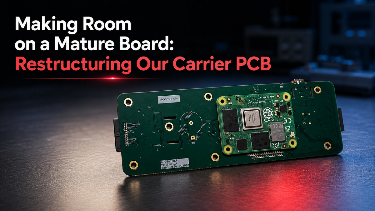
Most of the interesting hardware work at Hoomanely isn't greenfield. The connected feeding bowl already had a working carrier board: a compute module doing the thinking, a precision load-cell front end doing the weighing, connectivity, power, the usual. The board did its job. So when two new product features landed on the roadmap — per-pet identification so the bowl knows which animal is at it, and an audio channel so an owner can trigger a feeding or water alert the pet can actually hear — the question wasn't "how do we design a board." It was the harder one: how do we add two subsystems to a board that already works, without breaking the one thing the whole product depends on.
That last part matters more than it sounds. The core of this product is the weight reading. Everything downstream — portion tracking, feeding-session logging, the numbers a user sees in the app — hangs off a clean signal from the load-cell chain. Any restructuring that added features but degraded weighing accuracy would be a bad trade, no matter how nice the features looked in a demo. So the whole exercise was framed less as "add capability" and more as "add capability while protecting the analogue measurement." That framing decided almost every call we made.
The trigger was a bus, not a feature
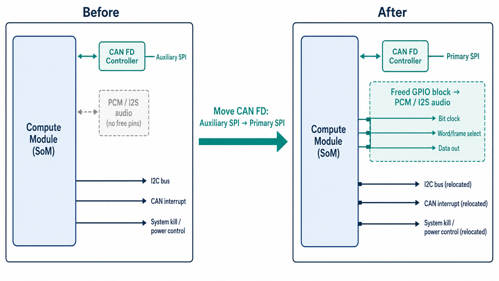
The audio feature needed a digital audio interface (I2S/PCM) off the compute module. That's a handful of dedicated pins, and they want to be contiguous and clean. The problem is that on a dense system-on-module carrier, the useful GPIO is already spoken for. There was no free block sitting around waiting for us.
What we did was a CAN FD controller parked on the module's auxiliary SPI controller — the cut-down secondary SPI peripheral, as opposed to the full-featured primary one. That placement had never been ideal; it was just what was free at the time. Moving the CAN FD controller onto the primary SPI controller did two things at once. It put the CAN traffic on the more capable, more predictable of the two SPI blocks, which is where that kind of link belongs anyway. And it freed up a contiguous run of GPIO — exactly the block the PCM audio interface wanted.
Here's the part worth writing down for anyone doing this kind of surgery: moving one interface is never local. Freeing that GPIO block meant the I2C bus, the CAN interrupt line, and the system power-control ("kill") signal all had to be relocated to keep the pin map coherent. None of those moves were hard individually. Collectively, they were the actual work. A single new peripheral rippled across a third of the pin assignments before the map settled again. If you budget "add audio" as a one-line change, the schedule will punish you. We budgeted it as a pin-map restructure, and it went fine.
Power was the real design decision
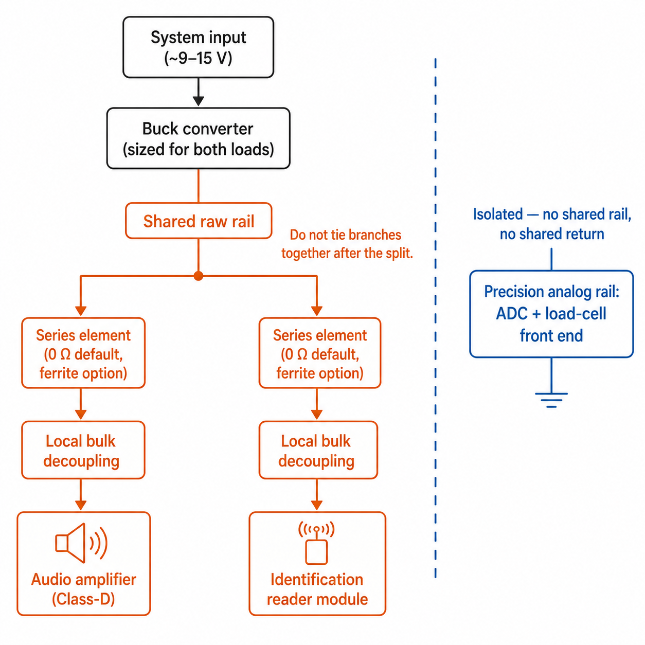
The two new subsystems — the audio amplifier and the identification-reader module — both wanted a roughly 5V supply. The lazy answer is two more regulators. We consolidated instead: one buck converter, sized to comfortably cover both loads on its own, feeding a single raw rail. Then that rail splits into two independently filtered branches — one for the amplifier, one for the reader module — each branch with its own series element and its own local bulk decoupling right at the load.
The series element is a small design hedge worth calling out. We populate a 0Ω resistor by default, but the footprint takes a ferrite bead. If bring-up shows the reader misbehaving on supply noise, or any coupling back toward the analogue side, we swap the part rather than respinning the board. It costs a footprint and buys an escape hatch. We left both branches with their own bulk caps precisely so they don't lean on each other during transients — the amplifier's current draw shouldn't be allowed to sag the reader's rail.
But the single most important power rule in the whole restructure is a negative one: none of this touches the ADC / load-cell rail. A Class-D amplifier is a switching load. Put its supply on the same rail as your precision analogue front end and its noise walks straight into your measurement. Since the measurement is the product, the audio-and-identification supply is a separate domain by design, kept off the analogue rail entirely. That's not a routing preference we'll relax under schedule pressure; it's a rule the architecture is built around.
Turning the new stuff off on purpose
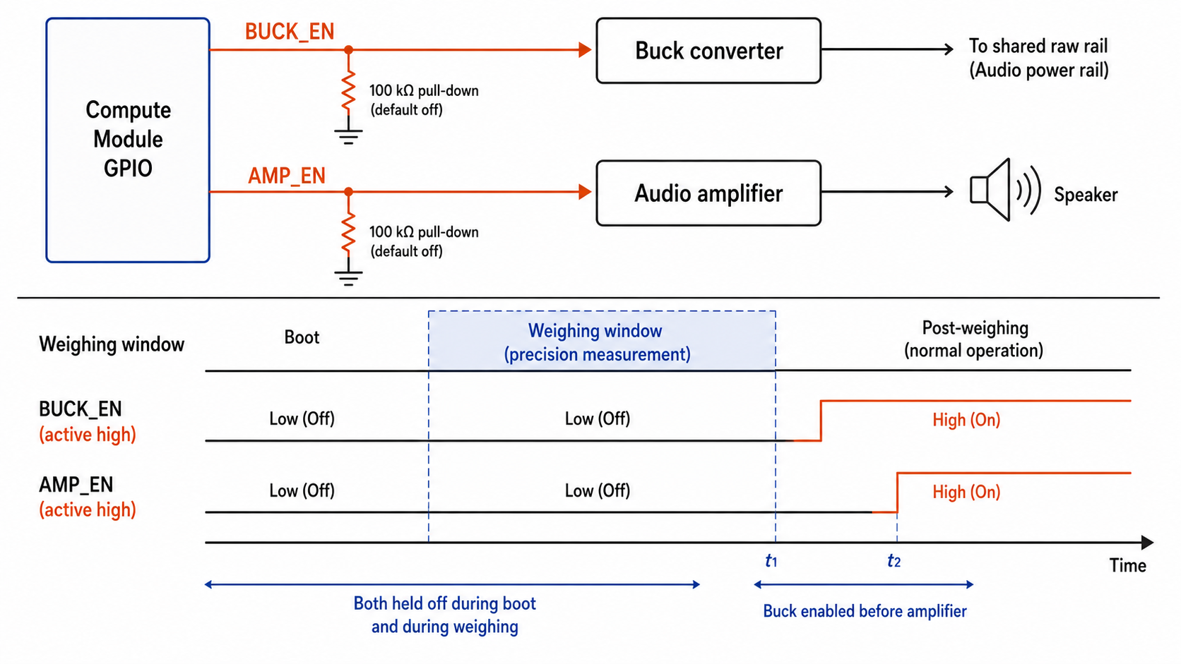
We gave the audio subsystem two independent enable signals rather than one — a separate enable for the buck and for the amplifier — and defaulted both to off with pull-downs at power-up. That's a little more copper and one more control line than the minimum, and it's deliberate.
Two reasons. First, boot: there's no reason for the audio domain to be live while the system is still coming up, and holding it off avoids pops and avoids drawing current before anything's ready to use it. Second, and more important, weighing windows. When the load-cell chain is taking a precision reading, we want the option to have the noisy switching neighbour genuinely quiet, not just idle. Independent enables let firmware sequence the audio domain around the measurement instead of the other way round. Power sequencing here is a first-class feature, not something we bolted on after noticing a problem on the bench.
Magnets, antennas, and keeping them apart
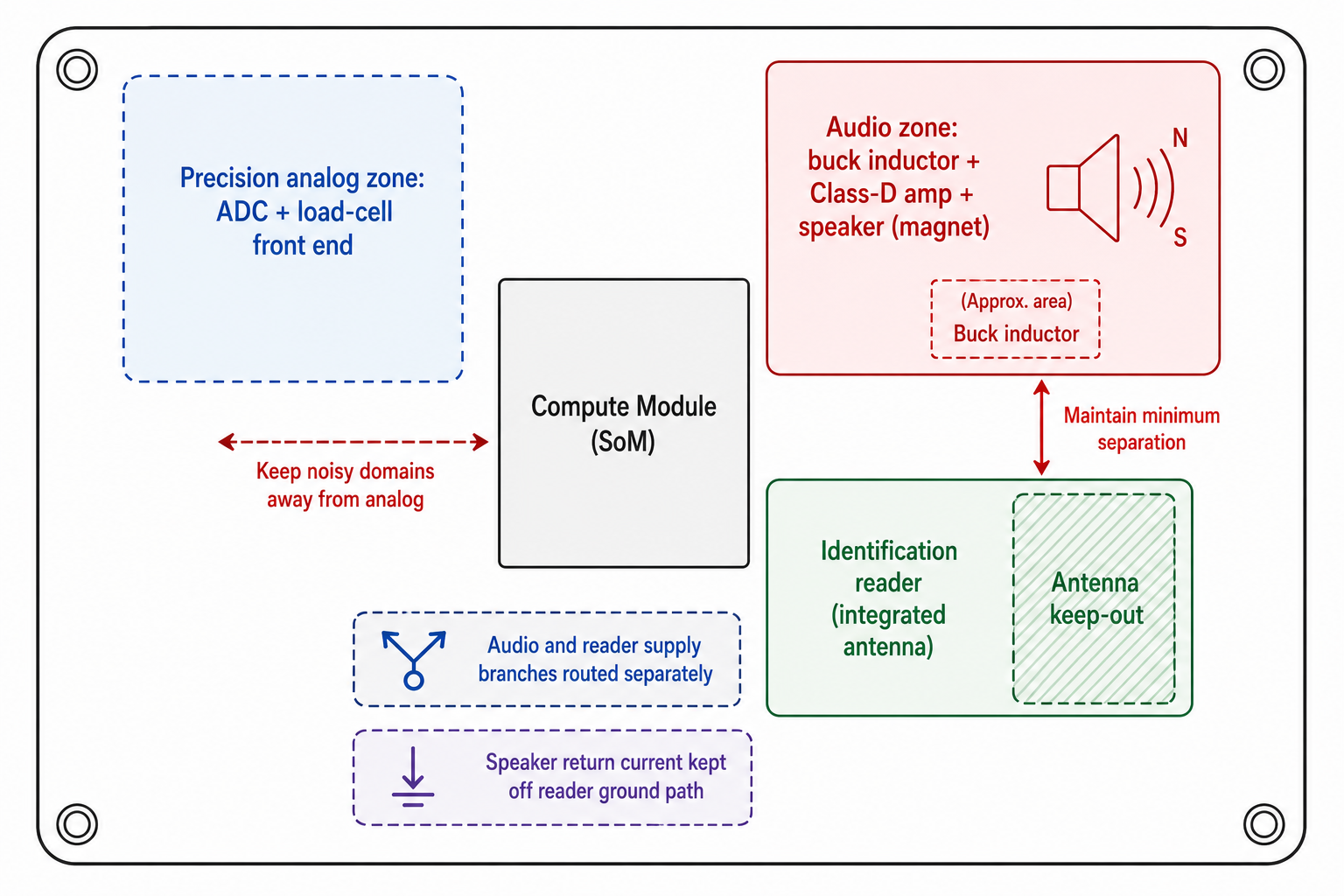
Two physical facts shaped the layout. The identification-reader we chose is a pre-certified module with an integrated antenna, which was a genuinely nice simplification — no custom antenna matching or tuning to design, so the schematic scope for it shrank to power, a serial interface, and an enable line. The cost of that convenience is a keep-out region around the module's antenna that you have to respect. The other fact is that the speaker has a magnet, and the audio buck has an inductor, and neither of those is something you want sitting next to an RF antenna.
So the placement discipline came down to a short list we held firm on: keep the speaker magnet and the buck inductor clear of the reader's antenna keep-out; keep the two supply branches routed separately after they split rather than sharing a trace or a plane pour; keep the speaker's return current off the reader module's ground path; and keep the whole audio-plus-identification cluster physically away from the ADC and load-cell section. EMI separation like this is cheap when you plan the floorplan around it and expensive when you try to patch it in after routing. We planned it in.
One honest note on the audio
We want to be straight about a limitation rather than oversell the feature. The amplifier runs single-supply in a bridge-tied configuration, and its headroom means the speaker will actually be driven a little under its nameplate power rating. That's fine — under-driven is safe, the speaker is never over-driven — but it does mean real-world loudness gets validated against the amplifier's measured output-versus-load behaviour, not calculated from Ohm's law and assumed. For an alert tone at close range this is more than adequate. We'd rather state the constraint than let anyone plan around a number the circuit won't hit.
What the restructure was really about
Adding features to a mature board is mostly an exercise in protecting what already works while you make room. The concrete moves were a bus reshuffle to free contiguous GPIO, a consolidated-but-isolated power branch, deliberate enable sequencing, and a floorplan that respects magnets and antennas. But the thread running through all of it was one constraint: the weighing signal chain is sacred, and every new subsystem had to earn its place without touching it. Keep that fixed, and the rest of the architecture more or less tells you what it needs to be.