The $47,000 Lesson: Why Your Working Prototype Isn't Ready for Market
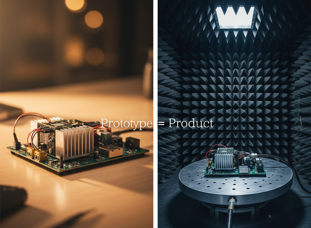
I've seen this story play out across the industry more times than I can count. A team builds a working prototype — everything looks perfect in demos, investors love it, morale is high, and excitement pushes everyone toward production.
Then certification testing happens.
Most prototypes fail on day one — radiated emissions over the limit, ESD killing the board, power integrity issues, and the harsh realization that a working prototype and a certifiable product are two completely different things.
At Hoomanely, I made sure we didn’t learn this the hard way.
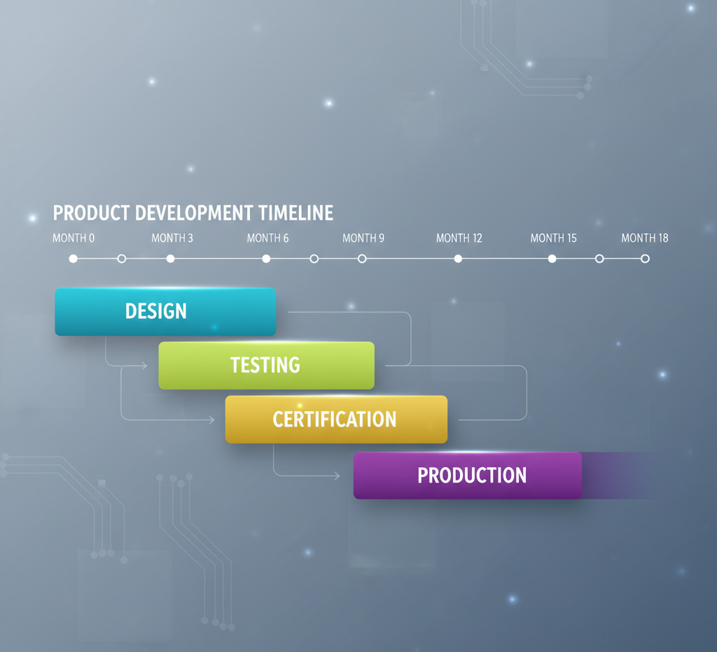
Instead of jumping straight from “it works!” to “let’s build thousands,” we implemented a structured hardware roadmap — from proof-of-concept to compliance to pilot production. We baked EMI strategy into the layout at prototype stage, performed pre-compliance scans early, validated components for long-term sourcing, and set up DFM reviews with our CM before locking the design.
The result?
We avoided redesign loops, passed certification smoothly, and reached a stable production-ready design without unnecessary delays or costs.
And that’s why I’m sharing the roadmap here — not from theory, but from real execution. If you're a founder, engineer, or someone who's curious about what really happens between a working prototype and a commercially certified, manufacturable product — this is the part nobody teaches in textbooks.
The Five Stages Nobody Warns You About
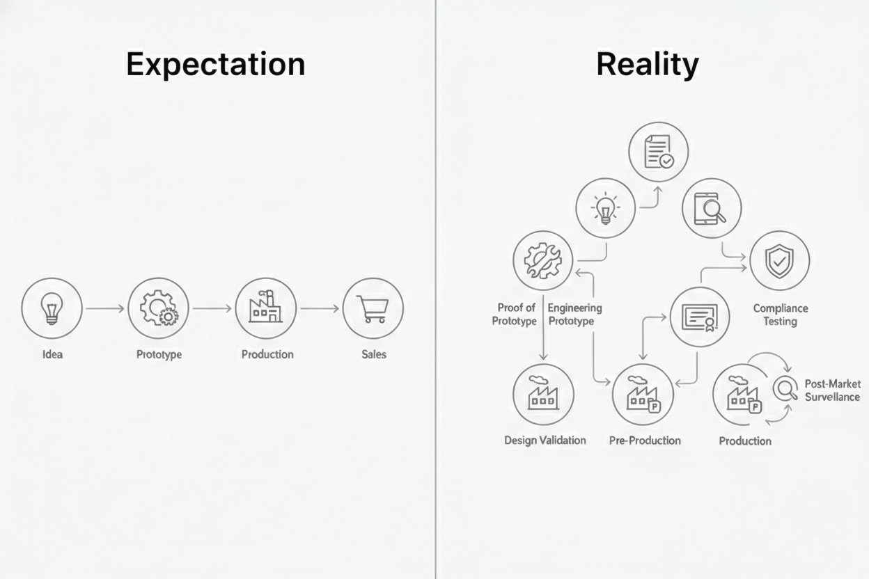
Let me break down what actually happens at each stage, and more importantly, what can go catastrophically wrong.
Stage 1: Proof of Concept (2-4 weeks)
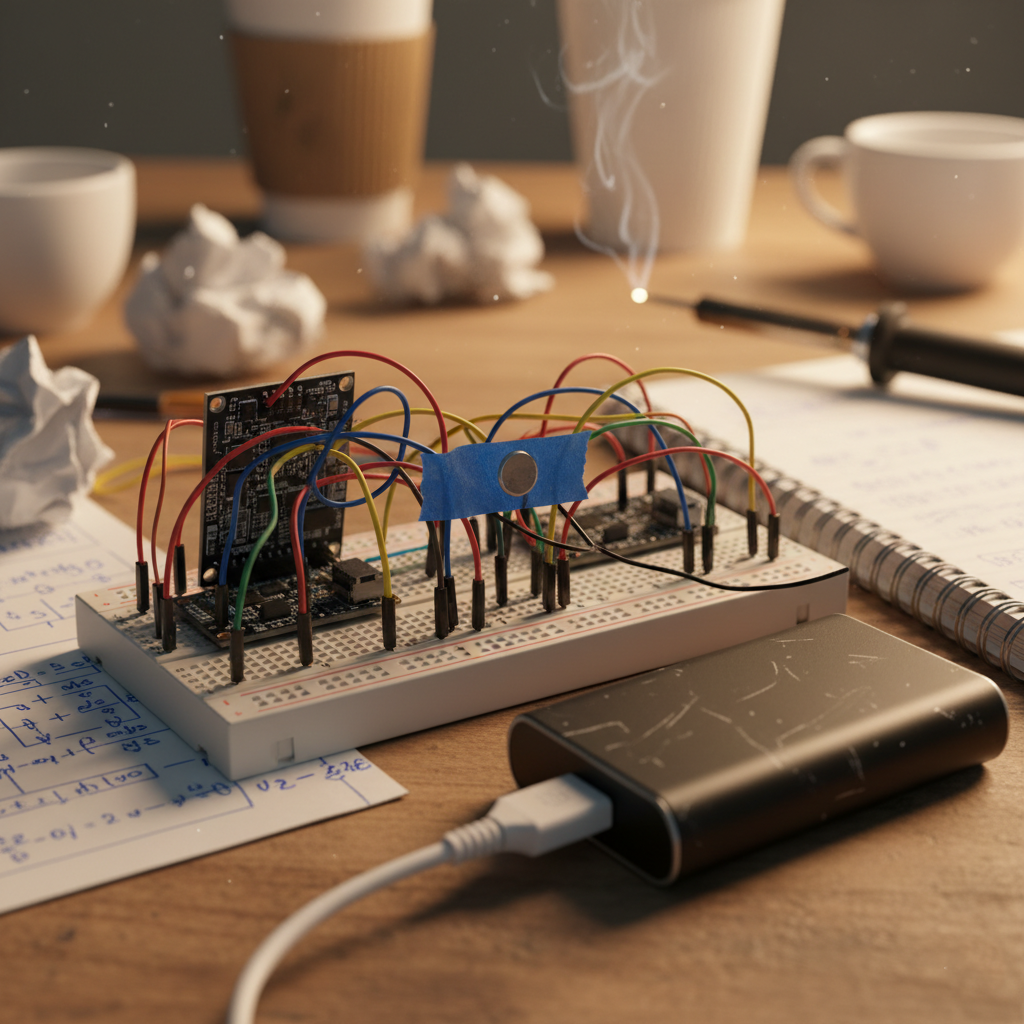
What it is: "Does this idea even work?"
This is where you breadboard the basic concept. It's held together with jumper wires and hope. Half the components are evaluation boards. The power supply is a lab bench unit with alligator clips.
What you're proving:
- Core functionality is technically feasible
- Key components can talk to each other
- Basic physics doesn't prevent this from existing
Red flags to watch for:
- Power consumption way higher than battery capacity allows
- Heat dissipation impossible in the target form factor
- Component costs already exceed target selling price
- Key sensors don't work in real-world conditions
Pro tip: Build the riskiest part first. If you're making a device with LoRa, GPS, and temperature sensing, build the LoRa communication first. It's usually the hardest part. Don't spend months on the easy stuff only to discover the core technology doesn't work.
Stage 2: Engineering Prototype (6-12 weeks)
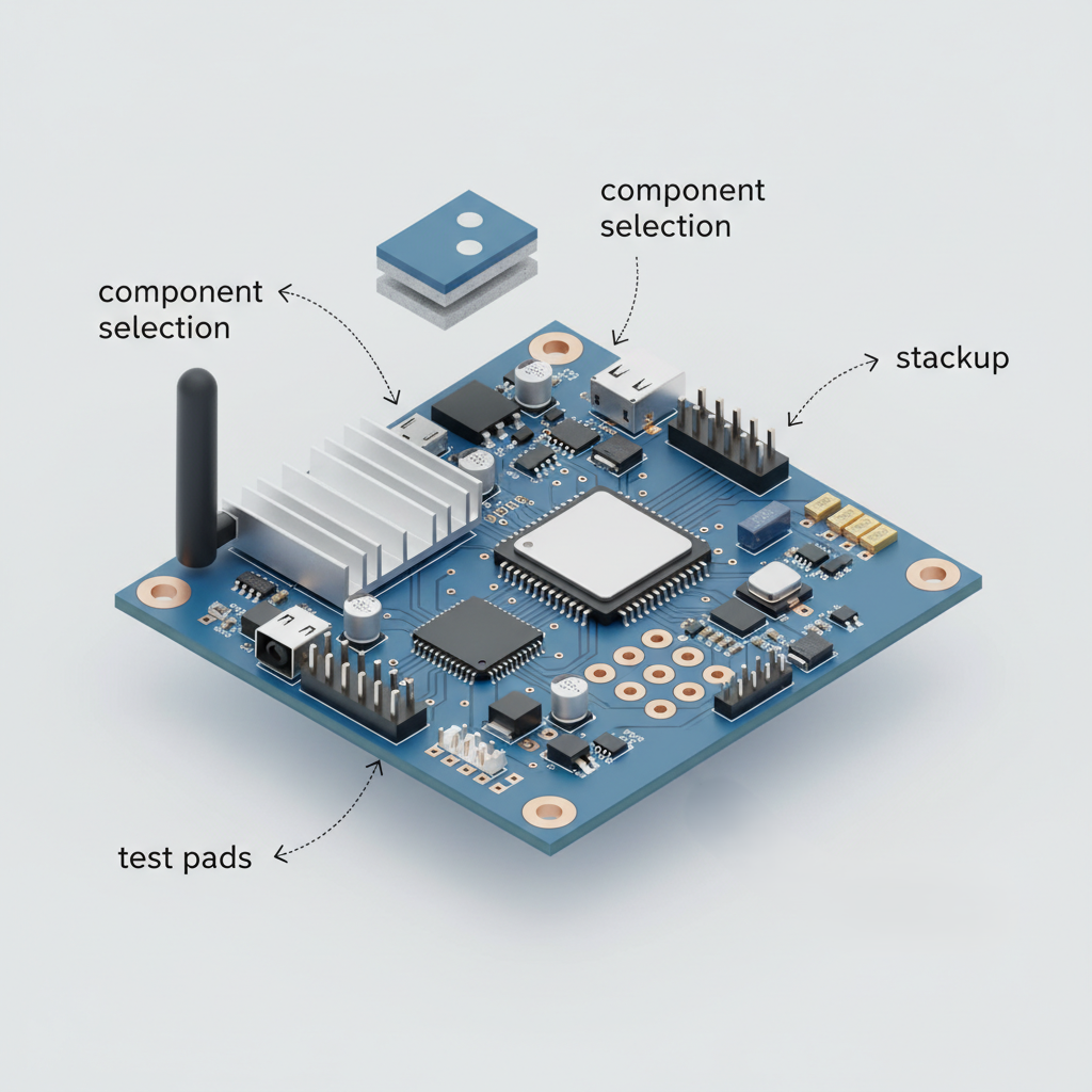
What it is: First "real" PCB design with actual connectors, proper power supply, mechanical enclosure concept.
This is where hardware engineers earn their salary. You're translating that messy proof-of-concept into an actual circuit board that somewhat resembles a product.
Critical decisions happening here:
- Component selection (choose wisely—changing later is expensive)
- Power architecture (battery? USB? Solar?)
- PCB stackup (2-layer? 4-layer? Rigid? Flex?)
- Microcontroller selection (this choice haunts you forever)
- Connector types and placement
What experienced engineers recommend:
Start thinking about certification requirements NOW, not later. EMI problems aren't fixed in stage 5—they're prevented in stage 2.
Choose components with good long-term availability. That perfect sensor chip with 6-week lead time? It'll be obsolete in two years, right when you scale production.
Design for test points. Future-you will need to debug production units. Present-you should make that possible.
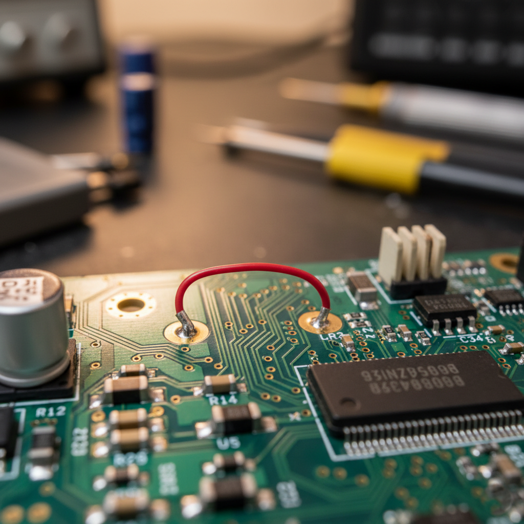
Leave space for "fixes." Your first board will have issues. If every square millimeter is packed, you can't bodge fixes to prove solutions before the next revision.
Expected outcome: A prototype that works well enough to show investors, do initial user testing, and identify major design flaws. Expect to build 10-20 units. Expect half of them to have issues requiring rework.
Stage 3: Design Validation Testing (4-8 weeks)
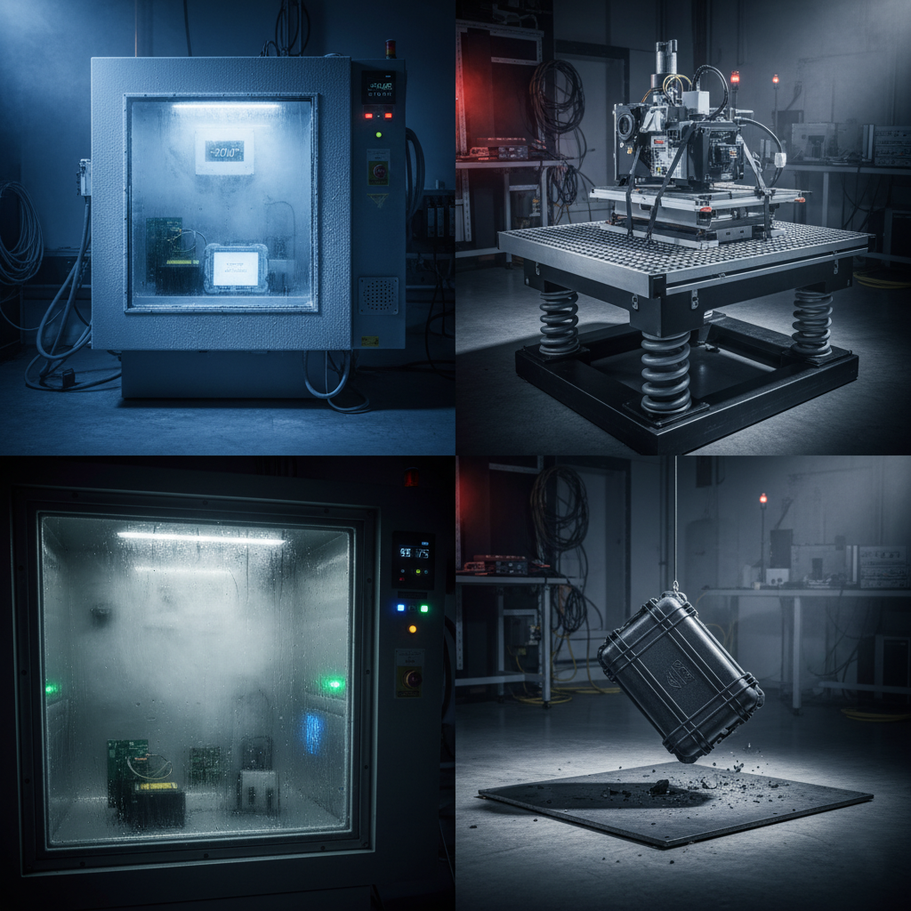
What it is: Torture testing your design to find everything that can go wrong, in a controlled environment where you can actually fix it.
This is the stage most startups skip. Don't skip this.
Tests you should run yourself:
Environmental stress testing:
- Temperature extremes (often -20°C to +70°C)
- Humidity exposure
- Vibration and mechanical shock
- Drop testing from various heights
Electrical stress testing:
- Power supply variations (what happens at 3.0V instead of 3.3V?)
- ESD simulation (touch every exposed metal with an ESD gun)
- EMI pre-compliance (radiated and conducted emissions)
- Power consumption under all operating modes
Functional edge cases:
- What happens when battery dies during data transmission?
- What if the user presses three buttons simultaneously?
- Can the device recover from every error condition?
Real story from industry experience:
Many companies build sensor devices that work flawlessly in controlled lab environments. But in field testing at industrial customer sites, units randomly reboot. After weeks of debugging, the culprit is often industrial motors creating power line noise that devices can't handle.
The fix? Better power supply filtering and software watchdog improvements. Cost in development: a few thousand dollars and one week. Cost if discovered after shipping thousands of units? A nightmare scenario no one wants to face.
Stage 4: Compliance Testing & Certification (8-16 weeks)
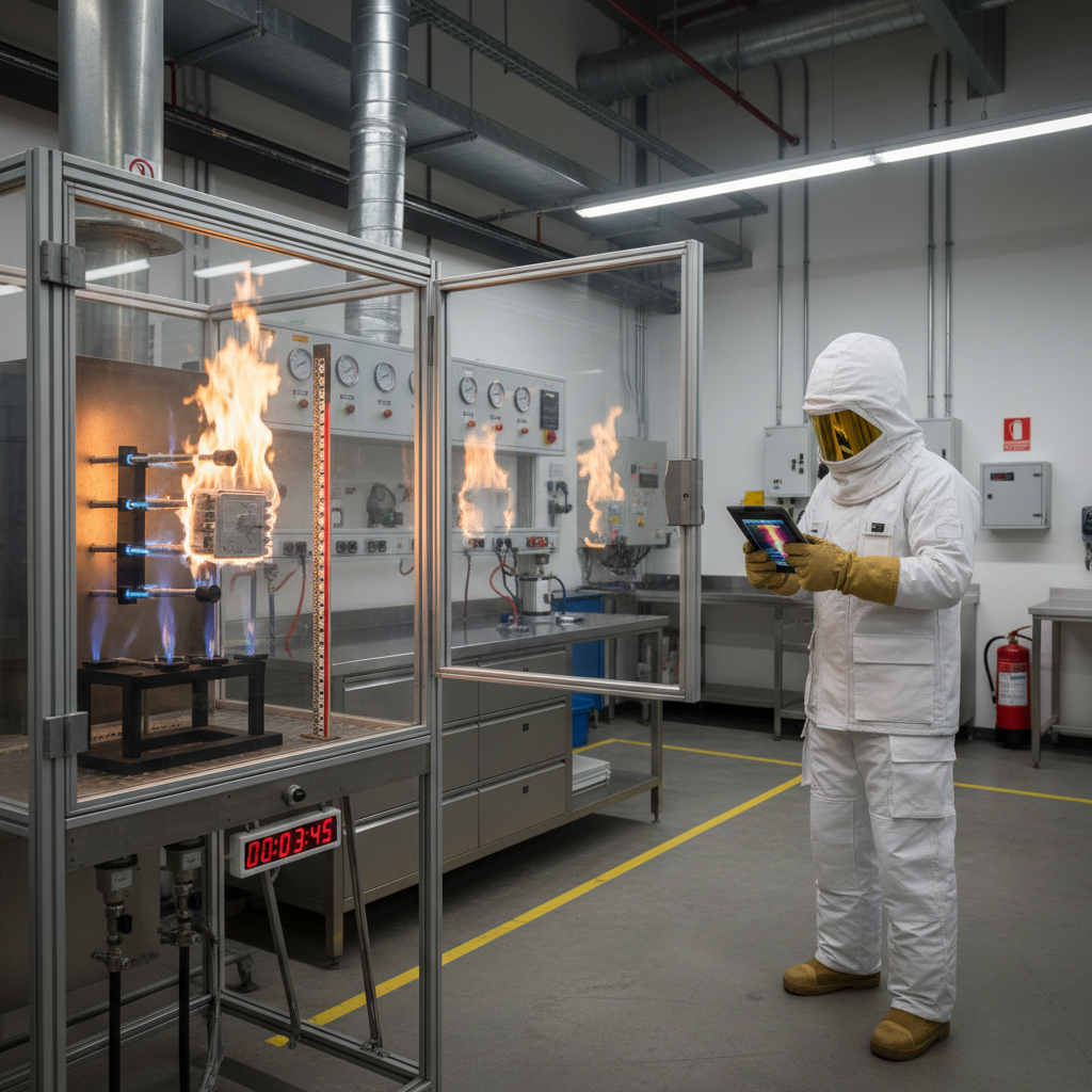
What it is: The gauntlet. Official testing by accredited labs to prove your device won't interfere with other electronics, won't hurt users, and meets legal requirements.
Main certifications you'll likely need:
FCC (USA) / CE (Europe):
- Radiated emissions testing
- Conducted emissions testing
- If you have a radio (WiFi, Bluetooth, LoRa): additional RF testing
- Cost: $5,000-$25,000 depending on complexity
Safety certifications (UL, TUV, CSA):
- Electrical safety
- Fire hazard testing
- Insulation testing
- Mechanical hazards assessment
- Cost: $10,000-$50,000 depending on product type
Battery certifications (if applicable):
- UN38.3 for shipping lithium batteries
- IEC 62133 for battery safety
- Cost: $8,000-$15,000
IP ratings (water/dust resistance):
- If you claim "waterproof" or "dustproof"
- Tested to IP67, IP68 standards
- Cost: $2,000-$8,000
The brutal reality of certification:
You don't just "pass" or "fail." You usually fail the first time, get a detailed report of every problem, fix them, and test again. Each re-test costs money.
Common failure modes encountered in the industry:
EMI failures: Your device radiates too much electromagnetic energy. Usually caused by:
- Poor PCB layout (we covered this in previous posts!)
- Inadequate shielding
- Cable radiation (yes, cables act as antennas)
- Switching power supply noise
ESD failures: Electrostatic discharge kills your device. Usually caused by:
- Inadequate ESD protection on connectors
- Poor grounding strategy
- Unprotected I/O pins
- Chassis design that channels ESD into sensitive circuits
Safety failures: Potential shock, fire, or injury hazards. Usually caused by:
- Insufficient isolation between mains voltage and user-accessible parts
- Inadequate wire gauge for current levels
- Sharp edges or pinch points
- Flammable materials too close to heat sources
A common pre-certification approach:
Before sending units to official labs, running pre-compliance testing at cheaper facilities or with rented equipment can find 80% of problems for 20% of the cost.
- EMI pre-scan with spectrum analyzer
- ESD testing with ESD gun (available for a few hundred dollars)
- Temperature testing in environmental chamber
- Mechanical stress testing
- Power supply variation testing
- All edge cases documented and tested
Stage 5: Design for Manufacturing (DFM) (4-8 weeks)
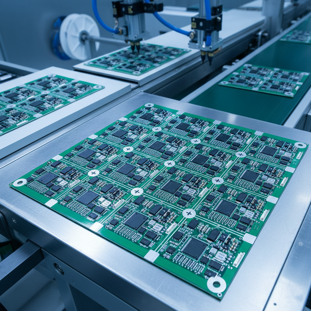
What it is: Taking your certified design and making it actually manufacturable at scale.
Your prototype might have hand-soldered components, bodge wires, and parts placed wherever they fit. Production needs different thinking.
DFM considerations:
Component placement:
- All components same side if possible (cheaper assembly)
- Similar components grouped together (faster pick-and-place)
- Test points accessible for automated testing
- Fiducials for automated optical alignment
Manufacturing tolerances:
- Can this be assembled by machines, not just by you?
- Are pad sizes standard for your CM's equipment?
- Can components handle reflow temperature profiles?
- Is your PCB thickness standard (1.6mm preferred)?
Test strategy:
- How will you test 100% of production units?
- JTAG/SWD programming and test access?
- Automated functional test fixture design
- Boundary scan testing for complex boards?
Cost optimization:
- Move to more common component packages
- Consolidate BOM (fewer unique part numbers = lower cost)
- Consider multi-sourcing for critical components
- Panel design for PCB fab efficiency
Real numbers from industry examples:
Engineering prototype BOM cost: $87 per unit After DFM optimization: $34 per unit At 10,000 unit volume: $19 per unit
Same functionality, smarter component choices and manufacturing processes.
Stage 6: Pilot Production (8-12 weeks)
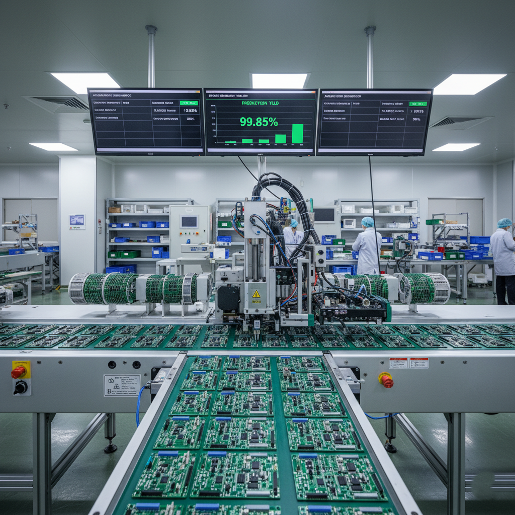
What it is: Building the first "real" batch (usually 100-500 units) on actual production lines to identify manufacturing issues before committing to high volume.
What you're really doing:
- Proving yield rates (what percentage pass testing?)
- Training CM staff on your product
- Validating test procedures
- Finding assembly issues the prototype didn't reveal
- Burning in software/firmware
- Creating work instructions and documentation
Things that will go wrong (trust me):
Some components won't be available (welcome to supply chain reality). You'll need approved alternate parts.
Assembly yield will be worse than expected. Your prototype was hand-assembled by experts. Production line operators see your design for the first time.
Test procedures you thought were clear will confuse the test technicians. You'll rewrite them multiple times.
Software/firmware bugs only appear at scale. That race condition that occurs 1 in 1000 boots? You'll see it 100 times in pilot production.
Success metrics:
- Assembly yield >95%
- Functional test pass rate >98%
- All critical components have approved alternates
- Test time meets production targets
- Documentation complete and validated
Stage 7: Production & Beyond

What it is: The "easy" part that's actually still hard.
You're building thousands or hundreds of thousands of units. New challenges emerge:
Supply chain management:
- Component lead times and availability
- Managing multiple vendors
- Quality control processes
- Inventory management
Quality monitoring:
- Field failure analysis
- RMA (return merchandise authorization) processes
- Continuous improvement based on real-world data
- Customer feedback integration
Regulatory maintenance:
- Certification renewals
- Responding to regulatory changes
- Documentation updates
- Post-market surveillance reporting
Cost optimization:
- Continuous cost reduction
- Process improvements
- Supplier negotiations
- Design tweaks for manufacturing efficiency
The Timeline Reality Check
From idea to first production units, here's the realistic timeline:
Startup with funding and focused team: 12-18 months Established company with resources: 9-12 months
Hobbyist or unfunded project: 18-36 months Complex medical or industrial equipment: 24-48 months
Notice these are much longer than most people expect. Here's why:
- Certification testing alone is 2-4 months, including fixing failures
- Supply chain delays add 4-8 weeks per board revision
- Testing takes longer than building
- "Just one more feature" adds months
- Everything takes twice as long as you estimate
The Cost Reality Check
Rough budget for bringing a moderate-complexity IoT device to market:
- PCB prototypes (3-4 revisions): $5,000-$10,000
- Components and assembly: $15,000-$30,000
- Test equipment and fixtures: $10,000-$20,000
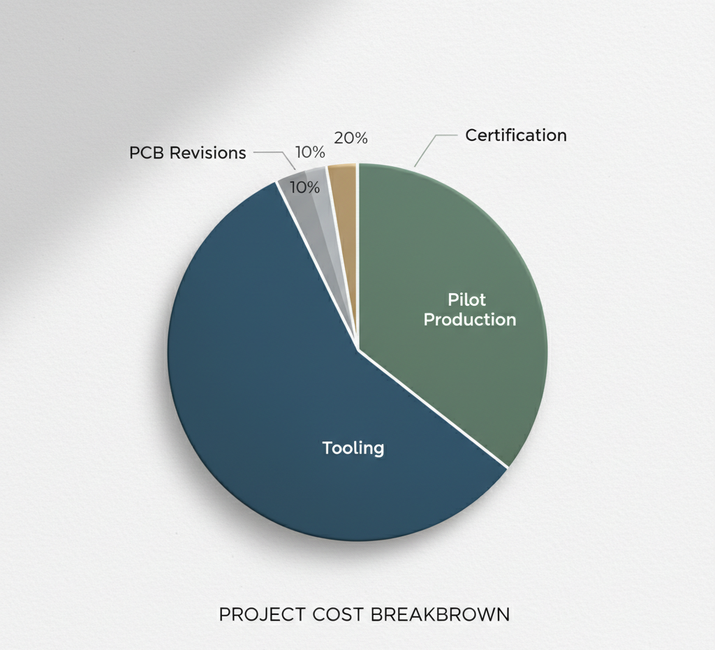
- Certification testing: $25,000-$75,000
- Pilot production: $50,000-$100,000
- Tooling and fixtures: $20,000-$50,000
- Engineering time (not even counting this): 6+ months
Total: $125,000-$285,000 minimum
And that's assuming everything goes reasonably well. Add 50% buffer for reality.
Key Lessons from the Field
Start with certification in mind. Every decision in early design affects certification later. EMI-conscious layout, ESD protection, safety isolation—these aren't optimizations, they're requirements.
Test early and often. Every stage of validation finds problems cheaper than the next stage would.
Component selection matters forever. That obscure sensor chip with amazing specs? It'll be obsolete when you scale. Choose boring, available, multi-sourced components.
Documentation isn't optional. Every test, every decision, every design change needs documentation. Certification audits demand it. Future debugging will need it.
Build relationships with your CM early. Your contract manufacturer isn't just a vendor—they're a partner. Get them involved in DFM reviews. Listen to their suggestions.
Budget 2x what you think for certification. And 3x the time. This applies across the industry.
Final Thoughts
Hardware is unforgiving. Software engineers can patch bugs after shipping. Hardware engineers can't. Once production starts, changes cost exponentially more.
But here's the thing: following this roadmap, as tedious and expensive as it seems, is still cheaper than skipping steps. Every shortcut comes back with consequences, usually during certification or in production when the cost to fix is at its maximum.
The industry has learned these lessons repeatedly. The roadmap isn't optional—it's how successful products actually make it to market.