The Engineer's Interface: Designing Silkscreen for Serviceability and Debug
A printed circuit board is more than a carrier for signals, it's a communication medium. At Hoomanely, we operate on a core truth: PCBs are read by humans just as often as they are powered by electricity. From the engineer debugging a prototype on the bench to the technician servicing a unit in the field, the board itself must speak.
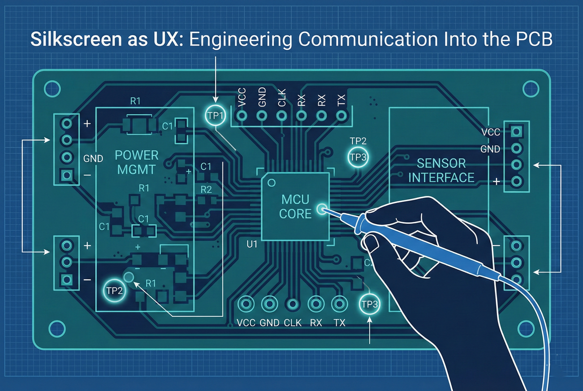
For these interactions, the silkscreen is not merely an aesthetic layer, it's the device's primary user interface. It transforms a complex, inscrutable artifact into an intuitive, serviceable machine. We treat silkscreen design as a deliberate exercise in user experience, knowing that clarity accelerates troubleshooting and ambiguity breeds error.
Serviceability first: the bench experience
When debugging live circuits, engineers need instant access to critical signals. Hunting for the right test point wastes time and risks probing the wrong locations. Clear test point labeling uses a TP prefix plus signal name, like TP_3V3 or TP_I2C_SDA, functionally grouped, sized at 0.8-1.0mm height for readability without magnification. Power rails get marked with voltage and current capacity, like "+5V (2A)" or "+3V3_CPU," immediately communicating rail voltage and capability. Differential pairs or communication buses get signal flow indicators, an arrow showing UART_TX direction, or CAN_H and CAN_L marking the high and low side.
Every component receives a unique reference designator printed adjacent to the component body, using standard prefixes, U for ICs, C for capacitors, R for resistors, L for inductors, D for diodes and LEDs, J for connectors, Q for transistors. Placement rules keep the designator visible after assembly, outside the component footprint, in consistent orientation, high contrast, and immediately adjacent with no ambiguity about which component it labels. Critical passive components include values alongside the designator, particularly useful for timing components, power supply filtering, and termination resistors.
Engineers troubleshooting power issues benefit from clear rail identification, net name labels near connectors, adjacent to regulator outputs, at high-current component power pins, and near test points, using a format like +5V_MAIN or +1V8_CORE. An engineer probing the board can instantly identify which power domain they're measuring, critical when multiple voltage rails are present.
Polarized components require clear orientation marking. Electrolytic capacitors get a plus symbol at the positive terminal plus a filled region at the negative terminal for visual redundancy. Diodes and LEDs get a cathode bar with a K or C label, eliminating ambiguity. Connectors get pin 1 marked with a square pad on the electrical layer plus a triangle or dot on silkscreen, with polarity marked for power connectors.
PCBs with distinct functional sections benefit from block labels in large text, like "POWER SUPPLY" or "CPU + DDR MEMORY," at 2-3mm height, readable from normal viewing distance without magnification. An engineer unfamiliar with the board can quickly orient themselves and identify the correct region.
Debug and development support
Development boards and prototypes include pin headers for probing and expansion, with every pin labeled with the signal name. Pin pitch often limits label length, so consistent abbreviations get used, TX not UART_TRANSMIT, SDA not I2C_DATA, documented in a reference guide. Dual-side labeling puts pin labels on both sides of the header when space permits, readable regardless of board orientation.
Configuration jumpers and DIP switches require clear documentation, jumper purpose labels indicating function, switch settings labeled with their meaning, and default settings indicated with a dot or text. Status LEDs are meaningless without labels, D1 for power confirming supply present, D2 for general status, D3 and D4 for UART transmit and receive activity, D5 for error condition, sometimes with color indication noted alongside.
PCB revision, date code, and part number get prominently displayed, typically near the board edge or in a corner, visible when the board is installed in the enclosure.
Manufacturing and assembly support
Optical assembly equipment requires fiducial markers clearly marked as FID1, FID2, FID3, eliminating ambiguity between fiducials and test points or vias during assembly setup. ICs with many pins need pin 1 marking through a dot, triangle, or emphasized corner, with polarity redundancy across silkscreen marking, soldermask opening asymmetry, and PCB copper pad shape all reinforcing the same information.
Components not installed in certain configurations get a DNP marking adjacent to the designator, or an OPT indicator for conditionally installed components. Critical assembly instructions get printed directly on the board, like sequencing notes when component height conflicts require a specific install order, or keep-out zone markings reserved for enclosure clearance.
Regulatory and compliance marking
Products requiring compliance testing carry standard location marks, CE marking, FCC ID, RoHS compliance indicator, WEEE symbol, sometimes with a QR code linking to online compliance documentation, user manuals, firmware updates, or support information. High-voltage or hazardous areas get warning symbols and safety notice text.
Aesthetic considerations that serve function
Company branding serves an identification purpose too, professional appearance reinforcing product authenticity, with the product name clearly identified, sized large enough to be visible without dominating the board. Soldermask color selection drives silkscreen contrast, white text on dark soldermask or black text on light soldermask. Font selection favors sans-serif fonts for clarity, with minimum stroke width around 0.15mm for manufacturability and minimum text height around 0.8mm for general labels.
Text size hierarchy matters:
- Large text at 2-3mm for functional block labels
- Product name
- Revision; medium text at 1-1.5mm for component designators and pin labels; small text at 0.8-1mm for test points and detailed notes
An engineer's eye naturally focuses on larger text first, so the most important information is most prominent.
Design process integration
Before releasing a design, a systematic review checks completeness (every component has a visible designator, all test points are labeled, power rails are identified, pin headers are fully labeled, polarity indicators are present), readability (text size meets minimums, nothing is obscured, orientation is consistent, contrast is maintained), accuracy (designators match schematic, pin labels match net names, voltage markings are correct, revision number is updated), and manufacturability (silkscreen doesn't overlap exposed copper, stroke width is within fab limits, spacing to pads is maintained).
Cross-functional review brings in the electrical engineer to verify technical accuracy, the firmware engineer to confirm debug features are adequate, the manufacturing engineer to validate assembly clarity, and the test engineer to ensure serviceability. Multiple perspectives catch issues a single designer might miss.
Real-world impact
Clear labeling reduces troubleshooting time from 15-20 minutes locating signals and cross-referencing schematics down to 2-3 minutes with signals clearly labeled at test points, an 80-85% time reduction for common debug tasks. Clear polarity and orientation marking cuts wrong-orientation assembly errors from an industry average of 1-2 per 100 components down to under 0.2 per 100, a 90% reduction. And field service efficiency improves as technicians identify and replace failed components faster, with clear designators aiding quick location and voltage markings aiding power troubleshooting, cutting service time 40-50% versus unlabeled boards.
Conclusion: engineering communication through silkscreen
Silkscreen design is human-factors engineering applied to technical hardware. By treating the silkscreen layer as a user interface for engineers, technicians, and operators, we transform PCBs from opaque objects into self-documenting, serviceable systems.
The investment is minimal, silkscreen adds no cost to manufacturing, requires no additional components, and introduces no electrical complexity. Yet the returns are substantial:
- Faster debug
- Reduced assembly errors
- Improved field serviceability
- Enhanced product professionalism
This is engineering empathy, designing not just for electrical function, but for human interaction. When the person debugging your board at 2am can instantly identify signals, quickly locate components, and confidently troubleshoot issues, that's when silkscreen succeeds as UX.