The Invisible Problem That Broke My First Design (And How You Can Avoid It)
Early in my career, I designed a circuit board that worked perfectly on my desk. But the moment we put it in a metal enclosure for testing, everything went haywire. Random resets. Glitchy behavior. Failed emissions testing.
The culprit? Electromagnetic Interference (EMI) – and a layout that ignored some fundamental rules.
Today, I want to share the layout patterns that transformed me from someone who "fixed EMI issues later" to someone who prevents them from day one.
What is EMI, Really?
Imagine your circuit board as a tiny radio station that doesn't mean to broadcast. Every trace carrying a signal is like a miniature antenna, radiating electromagnetic energy. When this energy interferes with other components (or nearby devices), you've got EMI.
The worst part? You can't see it. Your circuit might work beautifully in testing, then fail spectacularly when regulatory testing begins. That's an expensive mistake.
The Three Pillars of EMI-Friendly Layouts
1. Stitching Vias: Building Electromagnetic Bridges
Think of a PCB as a multi-story building. Different layers need to communicate and share a common electrical reference – that's where stitching vias come in.

The golden dots you see are stitching vias - small plated holes connecting ground planes across layers
What they do: Stitching vias are small plated holes that connect ground planes on different layers, creating a low-impedance path for high-frequency currents.
The key insight: Place them around the perimeter of your board and near high-speed components. I typically place stitching vias every 1/6th of a wavelength (for most digital designs, that's roughly every 10-20mm at high speeds).
Real impact: In one project, adding a grid of stitching vias around a WiFi module reduced radiated emissions by 8 dB – enough to pass certification without expensive shielding.
2. Ground Planes: Your Invisible Shield
If I could give one piece of advice to every hardware designer, it would be this: never underestimate the power of a solid ground plane.

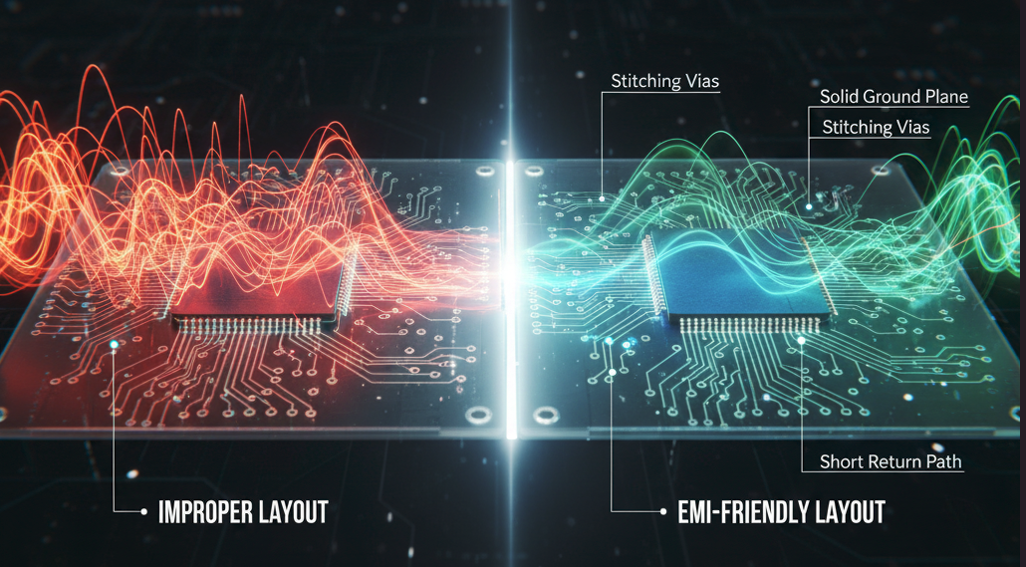
Good design (left): Continuous ground plane with smooth current flow. Bad design (right): Broken plane forcing chaotic current paths
What it does: A continuous ground plane on at least one layer (preferably multiple) provides:
- A low-impedance return path for signals
- Natural shielding against radiated emissions
- Heat dissipation
The mistake I see most: Breaking up the ground plane with traces or cutouts. Every time you split a ground plane, you force return currents to take longer paths, creating loop antennas that radiate EMI.

A well-designed PCB showing a continuous ground plane, proper decoupling capacitor placement, and organised high-speed traces
Best practice: Keep your ground plane as continuous as possible. If you must route signals on the ground layer, use the next layer or accept that you're creating a potential EMI source.
3. Return Paths: The Current's Journey Home
Here's something that surprised me early on: current doesn't just flow through your signal trace – it flows in a loop.
For every signal going from point A to point B, there's a return current trying to get back to the source. At high frequencies, this return current wants to flow directly beneath your signal trace (it takes the path of least impedance, not resistance).

Good design (left): Return current flows smoothly beneath signal trace. Bad design (right): Ground plane gap forces return current to detour, creating large EMI-radiating loops
The golden rule: Keep signal traces close to their return plane, and never let ground planes have gaps under high-speed signals.

Notice how the signal trace (highlighted) has a clear, uninterrupted ground plane beneath it for optimal return path
Example: I once debugged a USB 2.0 design that randomly failed enumeration. The issue? A 10mm gap in the ground plane right under the differential pair. The return current had to detour around the gap, creating a large loop area that radiated and picked up noise. Fixing the ground plane solved it instantly.
The Power Integrity Connection
There's a fourth pillar I'd add: decoupling capacitor placement.
Place your decoupling capacitors as close to the power pins as possible, with vias connecting directly to the power and ground planes. This creates localized low-impedance paths for high-frequency switching currents.
Poor decoupling placement forces these currents to travel across your board, creating both noise and EMI.

Same PCB design: Left shows the physical board, Right visualizes the electromagnetic activity with proper EMI management
The Checklist I Use on Every Layout
Before I call a layout "done," I verify:
- ✅ Continuous ground planes with minimal breaks
- ✅ Stitching vias every 10-20mm around the board edge
- ✅ High-speed signals have clear return paths underneath
- ✅ No ground plane gaps under critical traces
- ✅ Decoupling caps within 3-5mm of IC power pins
- ✅ Differential pairs stay close together (tight coupling)
Why This Matters Beyond Just Passing EMC Tests
EMI-friendly layouts don't just help you pass regulatory testing – they create more reliable, noise-resistant products. They reduce crosstalk, improve signal integrity, and often solve those mysterious "glitches" that are impossible to debug.
In my experience, spending an extra day on EMI-conscious layout saves weeks of debugging and potential board re-spins later.