LPDDR4 routing guidelines: stackup, impedance, length matching
LPDDR4 routing is decided before the first trace is drawn. The SoC vendor gives you four numbers that drive everything else: 40 ohm single-ended and 80 ohm differential targets with a plus or minus 10 percent window, a total route delay ceiling near 250 ps, and intra-pair skew limits of 0.75 ps on the clock and 1.5 ps on the strobes. Those numbers are only reachable if the stack-up was built for them, which is why a layer count and a dielectric table are the first LPDDR4 decisions, not the last.
This post walks through what the manufacturer guidelines actually ask for at 3733 MT/s: how to pick the stack-up, where the impedance tolerance gets spent before routing even starts, how to match on delay rather than physical length, and when the address and command bus needs a balanced T instead of a daisy chain.
The short version
- Every LPDDR4 signal belongs on a stripline layer with a solid plane on both sides, which is why a 3733 MT/s design lands on 10 or 12 layers rather than 6.
- The impedance target is 40 ohm single-ended and 80 ohm differential with a plus or minus 10 percent window, and dielectric constant tolerance alone can eat 4 to 5 percent of that window before the etcher touches the panel.
- Matching is specified in picoseconds, not mils: at roughly 7.1 ps/mm on an inner layer, a 1 mm length error on one DQ line is a 7.1 ps timing error, and the clock pair allows only 0.75 ps of intra-pair skew.
- The address and command bus feeding two channels of one DRAM wants a balanced T, with the split placed so both branches carry equal delay and each stub stays short enough to avoid becoming a reflection source.
Stack-up comes before routing, not after
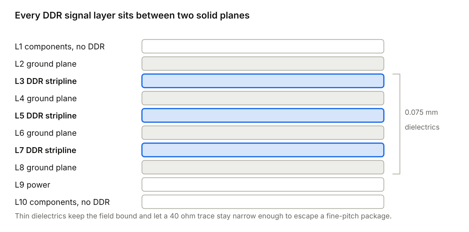
The first thing a manufacturer layout guide asks for is not a trace width. It is a layer structure in which every DDR net can run as a stripline, sandwiched between two uninterrupted reference planes, with no DDR routing on the outer layers at all. Once you accept that rule, the layer count stops being a cost decision and becomes an arithmetic one.
A 32-bit LPDDR4 interface carries four byte lanes, four strobe pairs, a clock pair, and a 6-bit command and address bus per channel. Those groups cannot share a routing layer freely, because byte lanes have to stay isolated from each other and the address bus has to stay isolated from the data. In practice that means two to three dedicated inner signal layers for DDR, each with its own plane above and below, which is how a design that would otherwise fit on 6 layers ends up at 10 or 12.
The outer layers are given up for a reason. A microstrip has air on one side, so its effective dielectric constant is lower, its propagation delay is different from an inner layer, and it radiates. Mixing a microstrip segment into a byte lane routed on stripline means the two halves of that net travel at different speeds, which turns a length-matched route into a delay-mismatched one. Keeping all DDR on stripline also gives the largest single EMI reduction available on the board, because the return current is captured between planes instead of coupling into the enclosure.
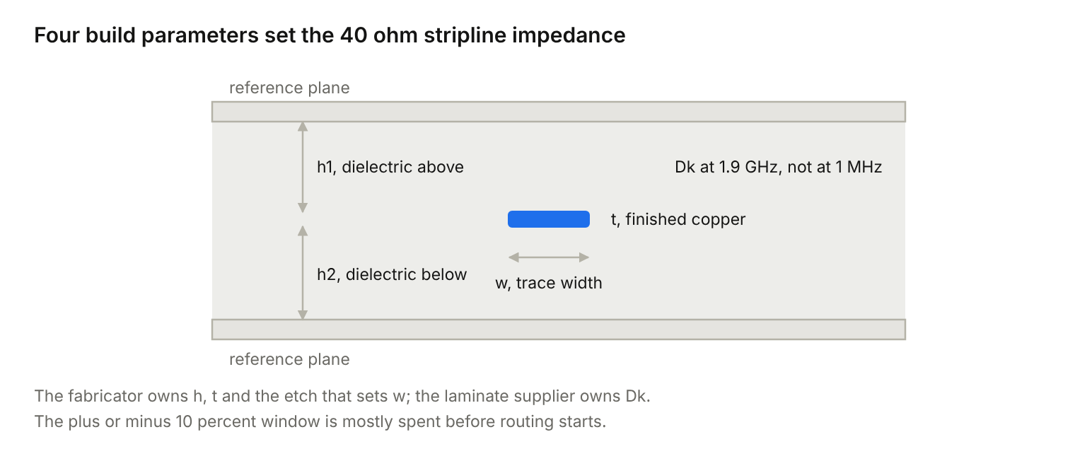
Dielectric thickness is the next binding choice. Thin dielectrics between the DDR signal layer and its references, in the region of 0.075 mm, let you hit 40 ohm with a narrow trace, keep the field tightly bound, and reduce crosstalk between adjacent nets. Thick dielectrics push the trace width up, which makes escape routing from a fine-pitch DRAM package impossible long before the impedance becomes a problem.
Glass weave style belongs in the stack-up specification too. Standard 1080 or 2116 weave has resin-rich and glass-rich regions on roughly a millimeter pitch, and a differential pair that happens to sit with one leg over glass and the other over resin picks up skew that no amount of serpentine correction can remove. Spread glass on the DDR dielectrics, plus routing pairs at 10 to 15 degrees off the panel axis or in a shallow zig-zag, is the standard mitigation and should be written on the fabrication drawing, not assumed.
Finally, the via structure. Above roughly 3200 MT/s, manufacturers start asking for microvias or back-drilled through holes, because the unused portion of a through via behaves as a resonant stub. On a board around 1.2 mm thick, back-drilling is not practical, so HDI with blind and buried vias becomes the only way to meet a 20 mil stub limit on the clock and address nets and 40 mils on the data nets. That decision has to be made with the fabricator before layout, since it sets the via spans that routing is allowed to use.
Impedance targets and where the margin goes
The targets are 40 ohm single-ended for data, strobes, clock and command lines, and 80 ohm differential for the strobe and clock pairs. The tolerance is plus or minus 10 percent, which sounds generous until you add up who spends it.
The mistake is to treat 10 percent as routing margin. It is a manufacturing window, and most of it is consumed by the fabricator before a single trace is drawn. The table below shows how a typical FR4 build divides it.
Source | Typical spread | Effect on 40 ohm | Who controls it |
|---|---|---|---|
Dielectric constant tolerance | Dk 3.8 plus or minus 0.15 | about 2 percent | Laminate supplier, stated at frequency |
Dielectric thickness tolerance | plus or minus 10 percent | 3 to 5 percent | Fabricator press cycle |
Etch tolerance on trace width | plus or minus 0.013 mm | 2 to 4 percent | Fabricator imaging and etch |
Copper thickness variation | plating spread on build-up layers | 1 to 2 percent | Fabricator |
Routing choices | neck-downs, pad entry, via transitions | 1 to 3 percent | You |
Added in the worst case those exceed the window, which is why fabricators quote impedance control as a controlled process rather than a guaranteed number, and why the coupon result matters more than the field solver result.
Two practical conclusions follow. First, take the dielectric constant from the fabricator datasheet at the frequency of interest, near 1.9 GHz for a 3733 MT/s interface, not from the 1 MHz catalog figure. The catalog number is usually optimistic by enough to shift the calculated width by several microns, which is real money against a 10 percent budget.
Second, give the fabricator the stack-up as a request, not a specification, and let them return the width and spacing that hits 40 ohm in their process. Their etch compensation and press behavior are known to them and not to you. The design rule you own is to keep the width constant everywhere it matters, because every change in width is a change in impedance, and a discontinuity in the middle of a 3733 MT/s net is worse than a 5 percent error applied uniformly.
Loss, incidentally, is rarely the constraint on a module-sized board. Over the 30 to 35 mm of route that the delay budget permits, even standard FR4 with standard copper foil stays well inside the insertion loss limit. The money is better spent on glass weave and plane integrity than on a low-loss laminate.
Trace width and spacing
Trace width is an output of the stack-up, not an input. For a 0.075 mm dielectric on either side of an inner layer with a dielectric constant near 3.8, a 40 ohm stripline comes out somewhere near 0.085 to 0.090 mm wide. You do not get to round that to a comfortable 0.1 mm, because the impedance moves with it.
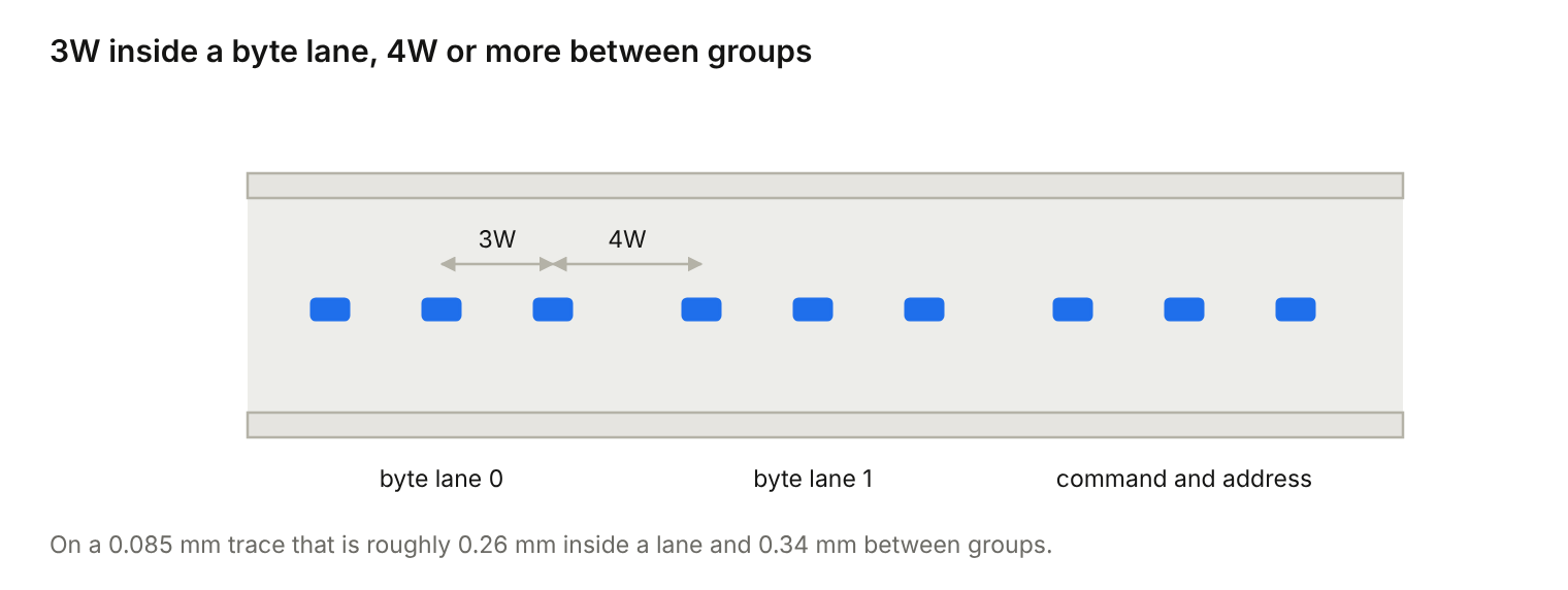
Spacing is where most of the crosstalk control lives. The usual manufacturer rule is 3W center to center within a byte lane, meaning three times the trace width, and 4W or more between different byte lanes and between the data group and the address group. On a 0.085 mm trace that is roughly 0.26 mm inside a lane and 0.34 mm between lanes, which is what drives the DDR routing channel width and therefore the placement of the DRAM relative to the SoC.
Strobe and clock pairs are routed to a differential spacing set by the 80 ohm target, and that spacing is held constant along the whole pair. Where a pair has to separate, for example to clear a via field, the separation should be short and symmetric, and the keep-out from neighboring single-ended nets should widen while the pair is uncoupled.
Neck-downs at the BGA escape are unavoidable and acceptable if they are short. The guidance is to keep any narrowed segment under roughly 1 mm so that the discontinuity is electrically short compared to the signal rise time. What is not acceptable is a neck-down that persists for several millimeters because a via was placed badly, since that is long enough to behave as a genuine impedance step.
Two more rules belong here because they cost nothing at layout time and are expensive later. Keep the width constant through the entire route rather than widening on a less congested layer, and never route a DDR net across a plane split or over a plane void, including the voids created by a dense via field in an adjacent layer.
Match on propagation delay, not on physical length
This is the rule that most often gets implemented wrongly, because every PCB tool defaults to matching in mils or millimeters. Manufacturer guidelines for LPDDR4 are written in picoseconds, and the two are only equivalent if every net in the group travels on the same layer with the same local dielectric.
An inner stripline on a dielectric constant of 3.8 propagates at roughly 7.1 ps/mm. An outer microstrip on the same board propagates nearer 6.0 ps/mm. If part of a byte lane escapes on a different layer than its neighbors, equal physical lengths are already several picoseconds apart, and the tool reports a pass.
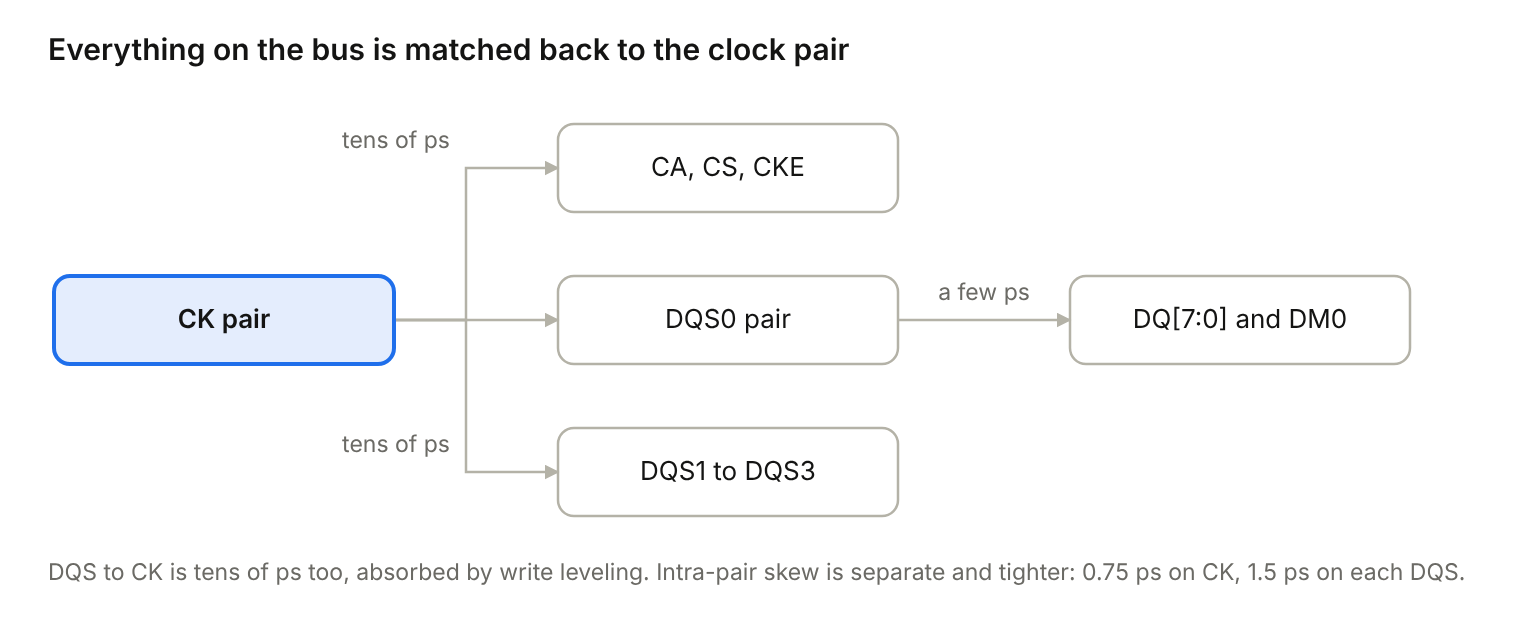
The matching groups and their typical allowances look like this.
Group | Matched against | Typical allowance |
|---|---|---|
DQ and DM within a byte lane | its own DQS pair | a few ps, tightest group on the bus |
DQS pair | CK pair | tens of ps, set by write leveling range |
CA, CS, CKE | CK pair | tens of ps |
Intra-pair, CK | itself | 0.75 ps |
Intra-pair, DQS | itself | 1.5 ps |
Total route delay, any net | absolute ceiling | about 250 ps |
Three configuration details decide whether those numbers mean anything. The SoC package delay has to be included, because the balls are not the die and the per-ball delay spread inside the package is comparable to the budget you are matching to. The DRAM package delay is usually excluded, because the DRAM vendor already accounts for it in the device timing. And the per-layer velocity has to be entered correctly in the constraint manager, which is the step worth verifying by hand before trusting any report.
Serpentines are how you spend the correction, and they have their own rules. Keep the amplitude at least 3W so the serpentine does not couple to itself, place it close to the source of the mismatch rather than at the end of the route, and never serpentine one leg of a differential pair to fix intra-pair skew. Intra-pair skew is corrected with a short bump at the point where the pair became asymmetric, typically at a via or a pin escape.
Via count is part of delay matching even though it never appears in a length report. Each layer transition adds delay and a small discontinuity, so manufacturer guidance caps the count, commonly two per data or strobe net and four per command or clock net, and asks that the count be identical within a matched group. Two nets of equal delay with different via counts are not equivalent.
Balanced T for the command and clock bus
Data is point to point. One DQ ball on the SoC drives one DQ ball on the DRAM, so there is nothing to branch. The command, address and clock nets are different, because one driver has to reach two loads whenever the interface is split across two channels or two ranks, and the topology you choose for that fan-out decides whether the bus closes an eye at 3733 MT/s.
DDR3 solved this with fly-by, a daisy chain past each load with a terminator at the far end, paid for with write leveling to absorb the growing flight time. LPDDR4 moved termination on die and dropped the external terminator, so fly-by loses its natural end point. For the short, two-load fan-out that a single LPDDR4 package presents, manufacturer guidance is a balanced T.
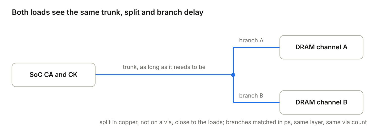
A balanced T is one trunk from the SoC to a split point, then two branches of equal delay to the two loads. The electrical argument is symmetry. Both loads see the same trunk, the same split and the same branch, so they see the same arrival time and the same reflection pattern, which means one set of timing numbers covers both and training does not have to compensate for an asymmetry that varies with temperature.
Four rules make the difference between a balanced T and a branch that rings.
- Put the split as close to the two loads as the escape allows. A long trunk and short branches is well behaved; a short trunk and long branches turns each branch into a stub seen by the other.
- Match the two branches on delay, not length, and tighter than the bus allowance. Branch to branch skew should be a small fraction of the CA to CK budget, because it is error you are adding on top of the SoC and DRAM uncertainty.
- Keep both branches on the same layer with the same width and the same via count. A T split across two layers is not balanced, whatever the length report says.
- Keep the clock pair on the same topology as the command bus it clocks. If CA splits at a T and CK does not, you have just created a skew that changes with every corner.
The split itself should be a simple tee in copper, not a via. A via at the split adds a stub at exactly the point where impedance matters most. Where the split has to change layers, do it before the tee on the trunk side, where there is one net rather than three.
One detail that catches people: the trunk impedance is seen looking into two parallel branches. A 40 ohm trunk feeding two 40 ohm branches sees 20 ohm at the split, so there is a step there no matter how carefully you route. Keeping the branches short relative to the signal rise time is what makes that step tolerable, which loops back to rule one. Manufacturer guidance usually states this as a maximum branch length rather than as an impedance rule, and the number comes from the DRAM package geometry and the chosen data rate.
The trunk carries one net and can be long; the branches carry the asymmetry and have to be short and equal.
The rules people break last
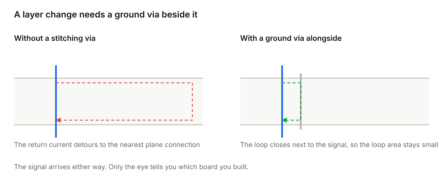
Return path comes first in importance and last in attention. Every layer transition on a DDR net needs a ground via beside it, placed close enough that the return current does not have to travel around the board to find a way between planes. Without it the signal still arrives, the eye just closes and nobody can say why.
Plane cuts inside the DDR region should be zero, not few. It is worth scripting that check rather than inspecting it by eye, because a cut introduced by a power rail routed on a plane layer is invisible on a signal layer view and is one of the few layout faults that reliably survives review.
Fiber weave was covered in the stack-up section, but it has a routing half: route differential pairs at a small angle to the panel axis, or zig-zag them, so each leg averages the same mix of glass and resin. This matters most for the clock pair, which has the tightest intra-pair allowance of anything on the bus.
Sequencing the layout saves the most time. Place the DRAM and fix the escape pattern before routing anything, route the clock pair first because it is the reference everything else matches to, then the command and address group with its T, then the byte lanes one at a time, matching each lane internally before moving on. Length correction comes last, after the via counts are frozen, because adding a via after matching invalidates the group.
What this lets EverBowl do
EverBowl(TM) runs its vision and sensor work on the application processor, and that work needs memory bandwidth that only an LPDDR4 interface at full rate provides. The routing discipline described above is what lets the processor hold several seconds of sensor and camera data in memory at once, which is the window the system needs before it can recognize which dog is at the bowl and decode a feeding event rather than a stray approach.
A memory interface that is marginal does not fail cleanly. It passes training on a warm bench and corrupts a frame three months later in a customer's kitchen, which is why the stack-up and the matching budget are treated as product requirements and not as layout preferences. The margin bought here is what makes the record trustworthy.
EverBowl does not diagnose. The value is the record, kept consistently enough that a veterinarian can see what changed and when. Learn more about the product at hoomanely.com.
Conclusion
Start with the stack-up, because the layer structure sets the trace width, the via strategy and the achievable impedance before you have any freedom left. Treat the plus or minus 10 percent impedance window as a fabrication budget rather than routing margin, and get the dielectric constant from the fabricator at frequency. Set your constraint manager to match on propagation delay with the correct per-layer velocity and the SoC package delay included, then verify that setup by hand once rather than trusting it forever. Route the clock pair first, give the command bus a balanced T with the split close to the loads, and freeze via counts before you correct any lengths. If one habit is worth carrying from this post, it is checking that the length report you are reading is actually a delay report.
FAQs
Can LPDDR4 at 3733 MT/s be routed on a 6-layer board?
Not while meeting the usual guidelines. Six layers does not give you enough inner signal layers with solid references on both sides to carry four byte lanes, the strobes, the clock and the command bus without putting some of it on the surface. Ten layers is the practical floor for a 32-bit interface at this rate, and 12 is more comfortable.
Why 40 ohm instead of the usual 50 ohm?
LPDDR4 drivers and on-die termination are specified around 40 ohm, so the channel is matched to the driver rather than to a generic convention. Routing a 50 ohm trace into a 40 ohm driver creates a mismatch at every end of every net, which costs eye height you cannot recover elsewhere.
Is length matching in mils ever acceptable?
Only when every net in the matched group runs on the same layer, with the same width, the same via count and the same local dielectric. That is a real condition on a well disciplined layout, but it is a condition to verify rather than assume, and the moment one net escapes on a different layer it stops holding.
Does the balanced T apply to the data lines as well?
No. Data, strobe and data mask lines are point to point between one SoC ball and one DRAM ball, so there is no fan-out to balance. The T applies to clock, command, address and the control nets that one driver shares between two channels or two ranks.
How much does the SoC package delay actually matter?
Enough that ignoring it can consume the entire matching budget. Per-ball delay inside a modern package varies by several picoseconds across the DDR interface, which is comparable to the allowance for data to strobe matching. Vendors publish the per-pin package delay for exactly this reason, and the constraint manager should be loaded with it.
What should go on the fabrication drawing?
The stack-up with dielectric thicknesses and tolerances, the dielectric constant at the frequency of interest, the impedance targets with tolerance, the glass style for the DDR dielectrics, and the via spans allowed on DDR nets. Anything binding that is left off the drawing is a parameter the fabricator is free to change.
References
- Texas Instruments, AM62x and AM62A DDR Board Design and Layout Guidelines (SPRAD66)
- JEDEC, JESD209-4 Low Power Double Data Rate 4 (LPDDR4) standard
- Micron, LPDDR4 and LPDDR4X design and routing guidance (TN-53-01)
- IPC, IPC-2141A, Design Guide for High-Speed Controlled Impedance Circuit Boards
- Texas Instruments, AM62A7 datasheet (SPRSP63)