Manufacturing Files Without Surprises

How We Made PCB Manufacturing at Hoomanely Predictable, Repeatable, and Fast
In hardware, the real deadline is not when the firmware compiles or the prototype boots.
The real deadline is when your manufacturer loads your files into their pick-and-place line — because that’s when surprises cost money.
At Hoomanely, we build connected pet hardware: weight-sensing bowls, pet trackers, BLE sensor nodes, and compute modules. Our product family shares a modular hardware ecosystem, and our priority is reducing time-to-market without sacrificing engineering rigor.
In our early builds, manufacturing “surprises” were our biggest source of delays:
- Missing or mismatched footprints on the CPL file
- CM asking for fiducials and tooling rails after file hand-off
- DFM feedback requiring footprint or silk changes → triggering re-spin
The fix was not “more documentation.”
The fix was creating a repeatable manufacturing file workflow.
This article documents the strategy I implemented that reduced PCB manufacturing surprises to almost zero, and consistently got us approved for production within 48 hours of file submission.
Step 1: CPL Accuracy — Designing for Machines, Not Humans

Most engineers think a Gerber export is enough.
In manufacturing, CPL kills more projects than Gerbers.
A CPL (Component Placement List) tells the factory exactly where every component goes (X/Y location, rotation, and reference designator).
Before optimization, our revisions looked like this:
| Issue | Impact |
|---|---|
| Rotation mismatches (especially QFNs, LEDs) | Wrong orientation → manual rework costs |
| Parts missing from CPL | Line stoppage → “Please resend CPL” emails |
| Center offset wrong for odd-shape components | Mis-pick errors on feeders |
What I implemented
1. Per-footprint origin and rotation rules inside our library.
Component rotation wasn't fixed after exports — it was fixed at the library level, eliminating recurring mistakes.
Example rule in library:
- LEDs → Origin placed at the optical center, rotation = 0° facing cathode left
- QFN → Origin at EP center, rotation = pin-1 heading up
2. JSON-based metadata attached to every footprint
{
"mpn": "AS5600L",
"mount": "SMD",
"rotation": 90,
"center": "pad1"
}
The CPL exporter reads these automatically.
No manual editing of spreadsheets.
Result → Reduced CPL rework requests from manufacturers to zero.
Step 2: Panelization — Designing with the Assembly Line in Mind
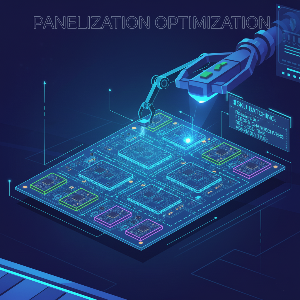
Panelization isn't just “put multiple PCBs on one sheet.”
Done right, it's a manufacturing optimization multiplier.
At Hoomanely, we have multiple product SKUs that reuse the same motherboard but different daughterboards/sensor modules.
Our panelization strategy:
| Goal | Implementation |
|---|---|
| Fast production trial builds | 3×2 test panel for prototype runs |
| Maximum pick-and-place efficiency | Shared edge rails with global fiducials |
| Modular product builds | Mix-panel of 2 SKUs on a single panel (only possible due to identical fiducials + datum points) |
Why it matters:
- Reduces feeder changeovers
- Faster assembly quoting (CM sees consistent panel format)
- Allows cost-optimized batching across SKUs
The assembly house should never panelize for you.
If they do it, you inherit their constraints, not your optimization.
Step 3: Fab Feedback Loop — No More “File Final Final V8”
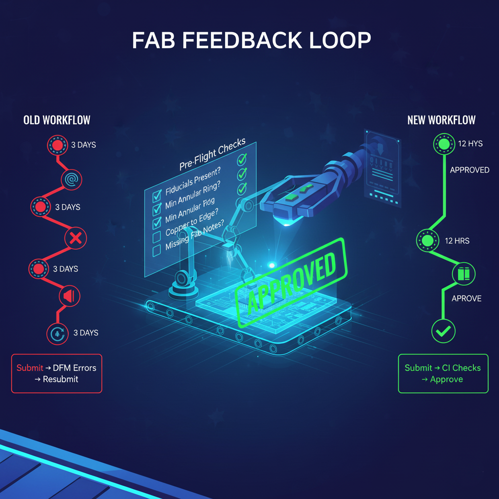
Before this process, every manufacturing cycle looked like:
Submit → wait 3 days → get DFM errors → re-export → re-submit → repeat
We changed it to:
Submit → feedback within 12 hours → one click regenerate → approved
How:
- Single source of truth document
(board spec + stack-up + via rules + impedance targets) - Pre-flight checks integrated into CI
- Missing fab notes?
- Fiducials present?
- Copper to edge spacing?
- Min annular ring?
- Manufacturer feedback codified back into templates and library
Example fab feedback → rule change:
| Fab Feedback | We Applied Permanently |
|---|---|
| “Your fiducials are too close to copper pour” | Added keepout rule: 2.5mm copper clearance around fiducials |
| “Side connectors require mechanical support pad” | Added auto-support pad rule to JST/board-edge footprints |
Every fabrication learning becomes a design rule, not a one-off fix.
Results
| Metric | Before Process | After Process |
|---|---|---|
| First-pass manufacturing success | ~70% | 100% on last 5 builds |
| Time from design freeze → CM approval | ~7–10 days | 48 hours |
| Manual CPL edits per build | 20–40 mins | 0 mins (fully auto) |
| CM back-and-forth email count | 6–10 threads | 1 (file received) |
Outcome:
We now go from design freeze to production-approval in 2 days.
No surprises. No re-spins caused by missing data. No manual Excel edits.
Final Thoughts
Engineering excellence isn’t the absence of mistakes —
it’s the presence of systems that prevent repeat mistakes.
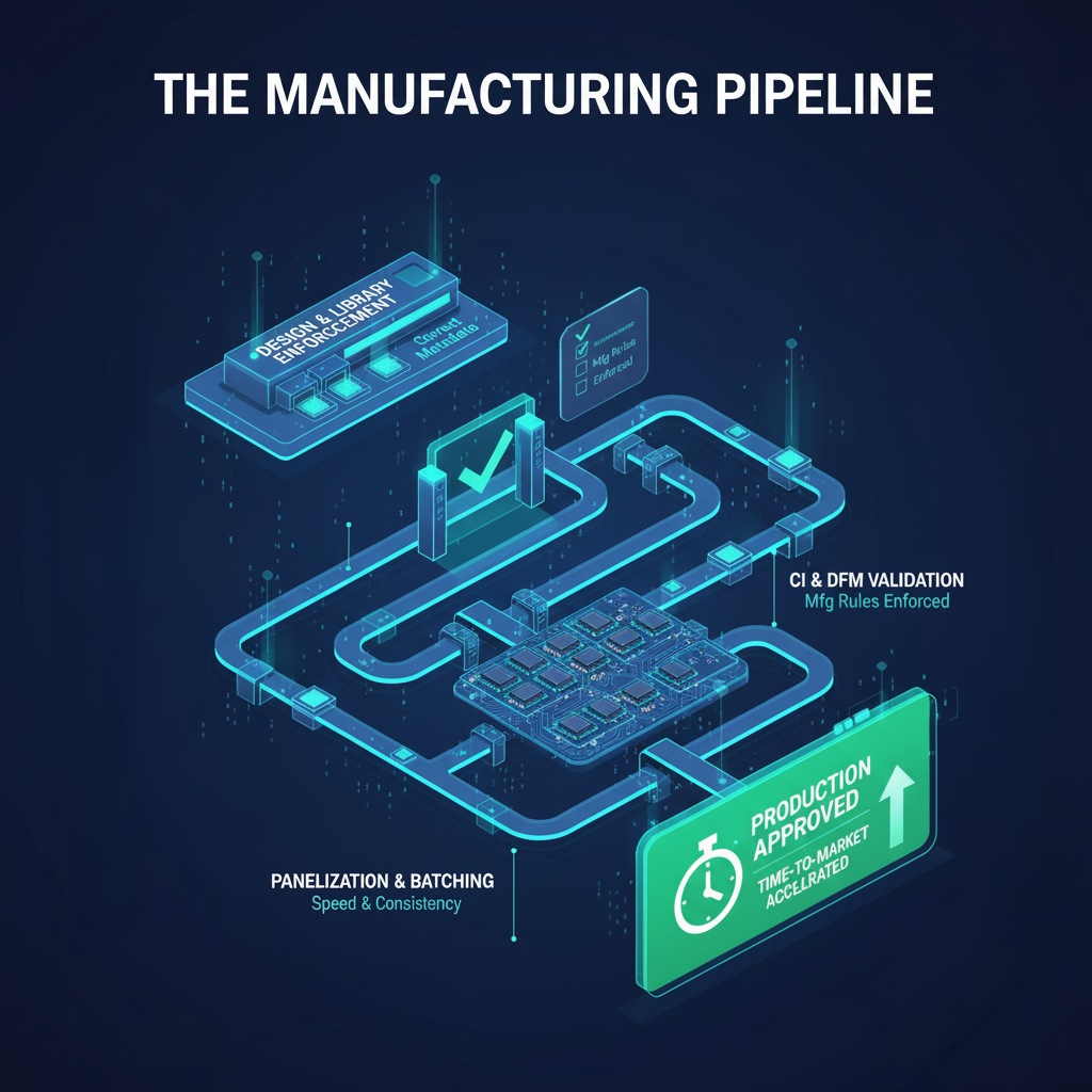
At Hoomanely, manufacturing is now treated as a software pipeline, not an afterthought:
- Libraries enforce correct metadata
- CI enforces correct manufacturing rules
- Panelization enforces speed and consistency
Hardware moves at the speed of how quickly you can learn from the last build.
By engineering the manufacturing workflow, not just the PCB,
we removed chaos from the build process and accelerated time-to-market