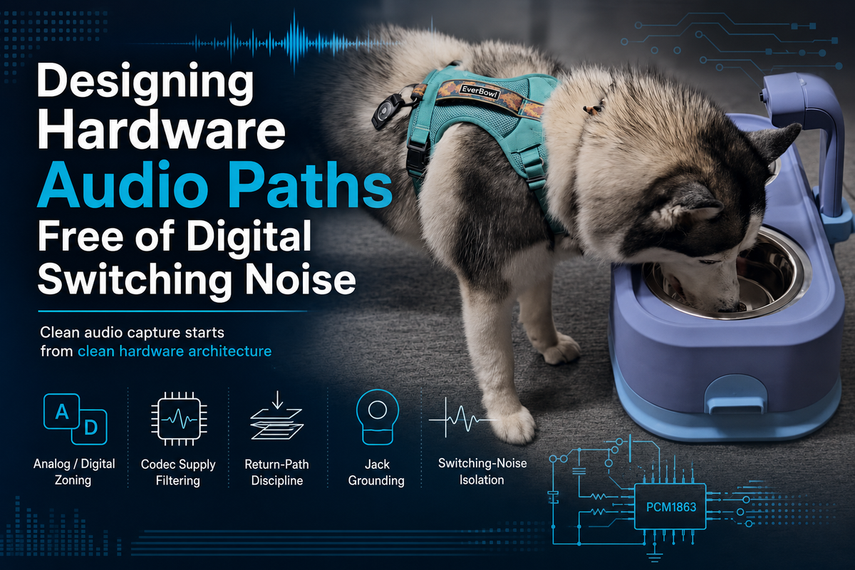
Designing Hardware Audio Paths Free of Digital Switching Noise
How mixed-signal architecture decides whether your product records clean audio or captures the noise of its own electronics
In a connected product, audio quality is often judged by the microphone, codec, and software processing algorithm. But many audio failures do not start in the microphone or the codec.
They start much earlier.
They start when the PCB designer places a switching regulator next to an audio trace, when a processor return current shares the same path as an analogue ground, when a digital interface crosses through a sensitive audio region, or when a connector shield is treated as a mechanical feature instead of an electrical boundary.
For products like EverBowl, where audio detection and recording are part of the user experience, the expectation is simple: the device should listen to the environment, not to itself.
The PCM1863 and similar audio ADC devices are capable of excellent audio performance, but the silicon can only work with the environment the PCB provides. A high-performance audio converter connected to a noisy power domain will still produce noisy recordings.
The challenge is not only selecting a good codec.
The challenge is designing the complete electrical environment around it.
Audio Quality Is Decided Before the Codec Receives the Signal
A common mistake in embedded audio designs is treating the codec as the "audio section" of the PCB.
The real audio section starts much earlier.
The microphone input, bias network, filtering components, codec supply, clock source, ground return, connector shielding, and PCB placement all become part of the audio system.
The PCM1863 does not know whether the noise arriving at its input is:
- actual environmental sound,
- power supply ripple,
- processor switching activity,
- DC/DC converter harmonics,
- USB noise,
- display activity,
- or digital communication interference.
It simply converts what it sees.
This changes the design approach.
Instead of asking:
"How do we remove noise after recording?"
The better hardware question is:
"How do we prevent unwanted energy from entering the audio path in the first place?"
A good audio PCB is designed around controlling current flow.
Every switching event creates current movement. Every current movement creates electromagnetic energy. The audio path becomes vulnerable when those currents are allowed to share the same physical routes.
Creating a Clear Analogue and Digital Boundary
The first discipline in mixed-signal design is separation.
Not isolation in the sense of physically cutting the PCB into two unrelated boards, but intentional zoning.
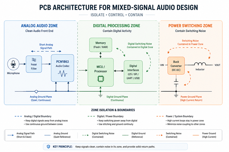
A good EverBowl audio architecture would typically have three electrical regions:
Analogue audio zone
Contains:
- Microphone input circuitry
- Input filtering
- PCM1863 analog pins
- Analogue supply filtering
- Audio reference components
- Audio connector interface
This region should experience minimal electrical activity.
Digital processing zone
Contains:
- MCU or processor
- Memory
- High-speed communication
- Display interfaces
- Wireless modules
- Digital audio interface
This region naturally creates noise because signals constantly transition between logic states.
Power conversion zone
Contains:
- Buck converters
- Battery charging circuits
- Switching regulators
- Inductors
- High-current paths
This is usually the loudest electrical region.
The mistake is not having these circuits on the same PCB.
The mistake is allowing their current paths to overlap.
A PCB does not understand schematic boundaries.
It only understands copper.
Codec Supply Filtering: Clean Power Creates Clean Audio
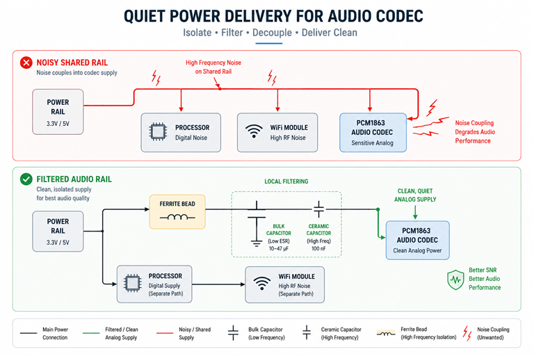
The PCM1863 depends heavily on supply quality.
Many designers connect the codec directly to the main 3.3V rail because the voltage is correct.
Electrically, that may work.
From an audio perspective, it can be problematic.
The main 3.3V rail may also power:
- Processor cores
- Wi-Fi modules
- Memory devices
- LEDs
- Communication interfaces
Every one of these loads creates current variation.
For example:
A processor transmitting data may suddenly change current consumption by hundreds of milliamps.
A wireless module may create periodic RF bursts.
A switching regulator may inject high-frequency ripple.
Without filtering, these disturbances appear on the codec supply.
A better approach is creating a quieter audio supply branch:
Main 3.3V Rail

        |
        |
    Filtering Network

        |
        |
 PCM1863 Analog Supply
Typical design considerations:
- Ferrite bead isolation
- Local decoupling capacitors
- Short supply routing
- Dedicated return path
The objective is not to create a completely separate power supply.
The objective is preventing noisy current from travelling through the same impedance seen by the audio circuit.
Return Path Discipline Matters More Than Ground Naming
One of the most misunderstood areas in mixed-signal PCB design is grounding.
Many designs create separate labels:
- AGND
- DGND
- PGND
and assume the problem is solved.
But the electrons do not follow labels.
They follow impedance.
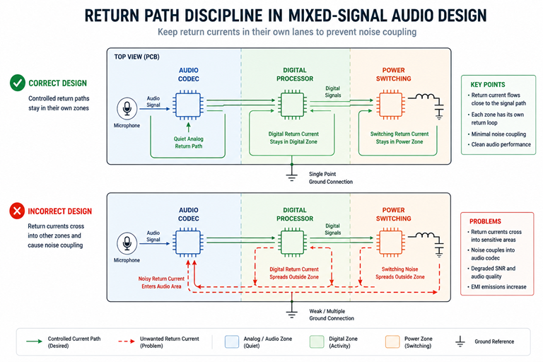
A digital processor return current will always find the lowest impedance path available.
If that path happens to pass through the audio reference area, the codec will see that disturbance.
A better approach is controlling where currents are allowed to flow.
For audio designs:
High-frequency digital return currents should remain close to their digital traces.
High-current power returns should avoid the codec region.
Audio reference currents should remain quiet.
A good PCB layout ensures:
- Digital signals have nearby return planes
- Power switching currents have dedicated loops
- Analogue audio traces are away from noisy return paths
The question is not:
"Where should ground connect?"
The better question is:
"Where will the return current travel during operation?"
Audio Jack Grounding Is an Electrical Boundary
Audio connectors are often treated mechanically.
A jack is mounted.
A few pins are connected.
The design is considered complete.
But connectors are where the outside world enters the product.
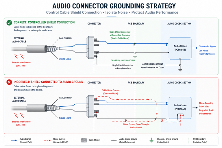
For audio systems, the connector creates several challenges:
- Cable shield currents
- External ground differences
- ESD events
- Cable movement noise
- Ground loops
The connector ground strategy needs intention.
A poor design may allow cable shield currents to flow through sensitive analogue ground regions.
This creates:
- Hum
- Buzzing
- Digital noise coupling
- Touch noise
A better architecture defines:
- Where the connector shield connects
- Where chassis ground connects
- Where signal ground references connect
The connector boundary should protect the internal audio system, not expose it.
Switching Noise Isolation: Keep Fast Energy Away From Slow Signals
Modern embedded devices are full of switching activity.
Examples:
- CPU clocks
- Memory buses
- PWM signals
- DC/DC converters
- Wireless transmissions
Audio is different.
Audio signals are small and continuous.
The PCB challenge is that a slow analogue signal and a fast digital transition do not coexist well.
A few practical rules help:
Keep switching nodes physically distant
The hot node of a buck converter can radiate significant noise.
Do not place:
- Audio traces
- Codec inputs
- Microphone bias circuits
near:
- Inductors
- Switching nodes
- Gate drive signals
Avoid digital traces crossing audio regions
A high-speed digital line crossing underneath an analogue input trace creates unwanted coupling.
Even if the signal works electrically, the audio quality may degrade.
Control clock noise
Audio converters require clocks.
Clock routing should have:
- Controlled impedance
- Short routing
- Stable return path
A noisy clock can directly appear as unwanted audio artefacts.
Designing the Audio Path as a System, Not a Component
The biggest lesson from embedded audio products is that the codec is rarely the failure point.
The surrounding architecture decides performance.
A clean EverBowl audio design would consider:
- Where microphone signals enter
- Where codec power comes from
- Where digital processing happens
- Where switching regulators operate
- How return currents move
- How external connectors interact with the PCB
Every decision either protects the audio path or exposes it.
The best audio designs are usually not the ones with the most filtering components.
They are the ones where unwanted noise never gets an opportunity to enter.
Practical Hardware Checklist for Noise-Free Audio Paths
Before releasing a mixed-signal audio PCB, verify:
- Is the analogue audio region physically separated from digital switching areas?
- Does the codec have a clean filtered supply?
- Are switching regulator loops kept compact?
- Are microphone traces short and protected?
- Are digital return currents controlled?
- Does the audio connector have a defined grounding strategy?
- Are clock signals isolated from analogue inputs?
- Are high-current paths separated from audio references?
- Can each subsystem be powered and debugged independently?
These decisions are made during PCB architecture, not during audio testing.
Final Thoughts
Clean audio is not created inside the codec.
It is created around the codec.
The PCM1863 can accurately capture what reaches its input, but the PCB decides what reaches that input.
A product that listens well is not only using a good microphone or a good ADC.
It is respecting the difference between noisy digital energy and sensitive analogue information.
In hardware architecture, the goal is not to fight noise after it appears.
The goal is designing the board so the noise never reaches the listener.
That is what separates a working audio board from a reliable product.