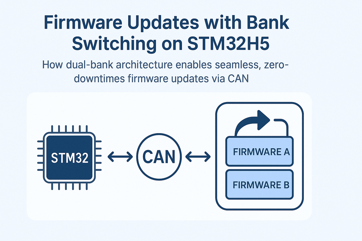
Firmware Updates with Bank Switching on STM32H5
How dual-bank architecture enables seamless, zero-downtime firmware updates via CAN
Firmware updates are crucial for modern embedded systems, enabling remote device maintenance, feature additions, and security patches without physical access. This post covers a production implementation on the STM32H562, which features a dual-bank flash architecture enabling seamless firmware updates through bank switching, optimized for CAN FD communication with 64-byte frame payloads. Key highlights: zero-downtime atomic updates, power-loss safe operation, and automatic rollback.
Bank configuration
// STM32H5 Dual-Bank Flash Configuration
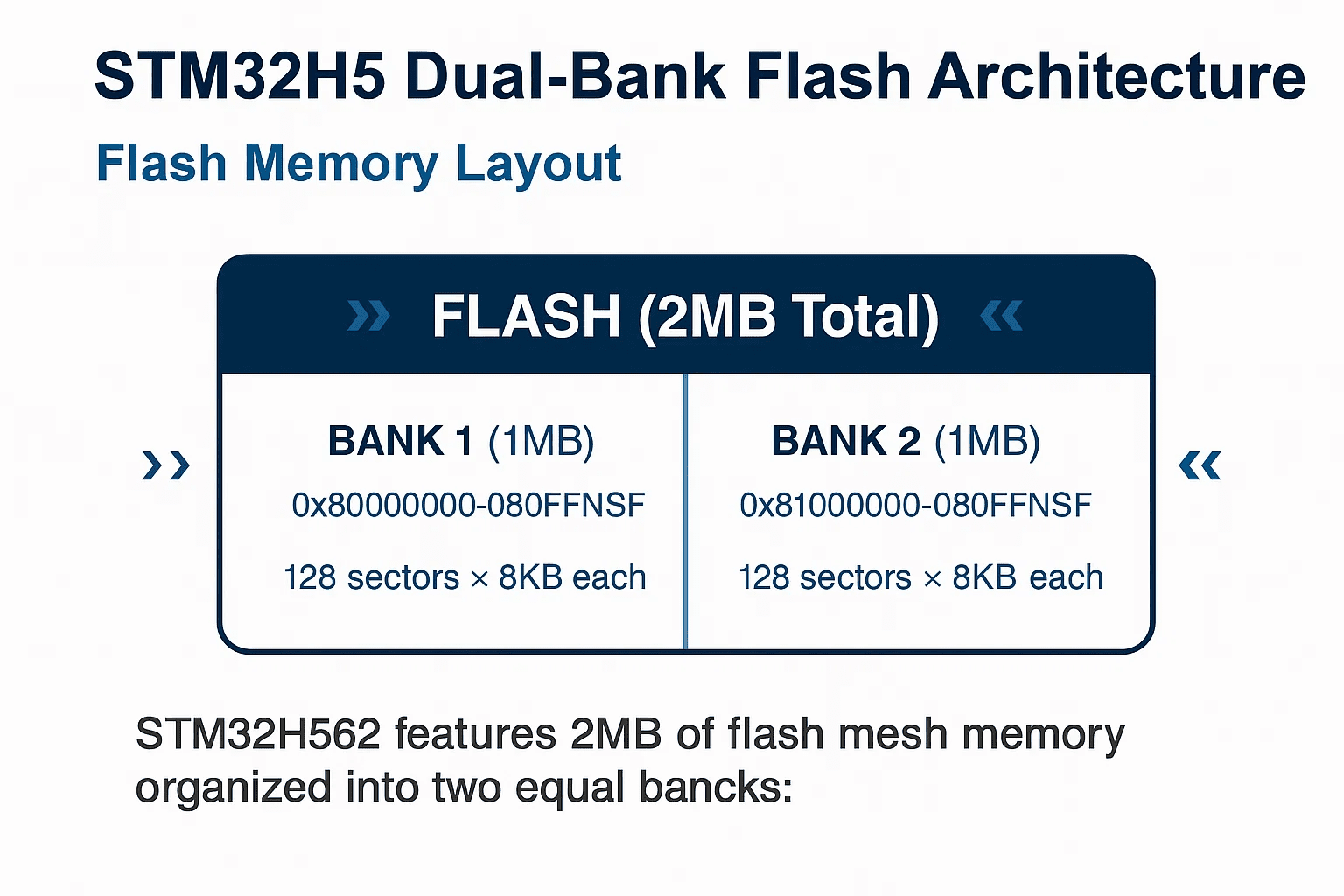
#define BANK1_BASE        0x08000000  // Bank 1 start
#define BANK2_BASE        0x08100000  // Bank 2 start
#define BANK_SIZE         0x00100000  // 1MB per bank
#define SECTOR_SIZE       0x00002000  // 8KB per sector

// Flash Layout per Bank
#define FIRMWARE_MAX_SIZE (BANK_SIZE - 2 * SECTOR_SIZE)
#define METADATA_OFFSET   (BANK_SIZE - SECTOR_SIZE)
The dual-bank architecture gives simultaneous read-while-write capability, 8KB sectors for fine-grained erase operations, hardware bank swapping via option bytes, and metadata storage in reserved sectors. This is the foundation for safe, atomic firmware updates.
The bank switching mechanism
STM32H5's bank switching is controlled by the SWAP_BANK bit (bit 31) in the Option Status Register. Toggle this bit and reset, and the hardware automatically remaps which physical bank appears at logical address 0x08000000, that's the mechanism that enables zero-downtime updates.
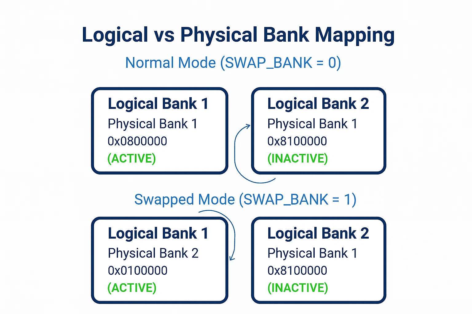
In normal mode (SWAP_BANK = 0), logical address 0x08000000 maps to physical Bank 1, logical 0x08100000 maps to physical Bank 2, and the system boots from physical Bank 1. In swapped mode (SWAP_BANK = 1), it's reversed. Your firmware always runs from 0x08000000, the hardware handles the mapping underneath.
error_t switch_bank(void) {
    // Unlock flash and option bytes
    HAL_FLASH_Unlock();
    HAL_FLASH_OB_Unlock();

    uint32_t optsr_cur = FLASH->OPTSR_CUR;

    // Toggle SWAP_BANK bit
    if (optsr_cur & FLASH_OPTSR_SWAP_BANK_Msk) {
        CLEAR_BIT(FLASH->OPTSR_PRG, FLASH_OPTSR_SWAP_BANK_Msk);
        printf("Clearing SWAP_BANK bit (Bank 2 -> Bank 1)\n");
    } else {
        SET_BIT(FLASH->OPTSR_PRG, FLASH_OPTSR_SWAP_BANK_Msk);
        printf("Setting SWAP_BANK bit (Bank 1 -> Bank 2)\n");
    }

    // Start option byte programming
    SET_BIT(FLASH->OPTCR, FLASH_OPTCR_OPTSTART);

    // Wait for completion and launch
    HAL_FLASH_OB_Launch();  // This triggers system reset

    HAL_FLASH_OB_Lock();
    HAL_FLASH_Lock();

    NVIC_SystemReset();  // Force reset if launch didn't trigger it
    return FU_OK;
}
The update flow
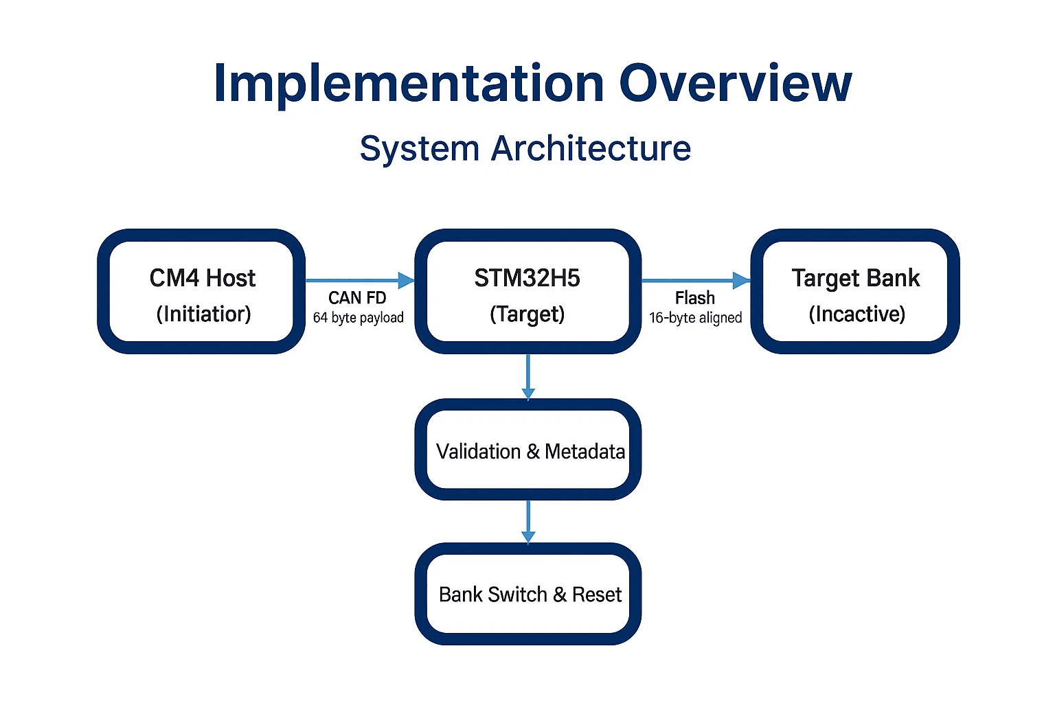
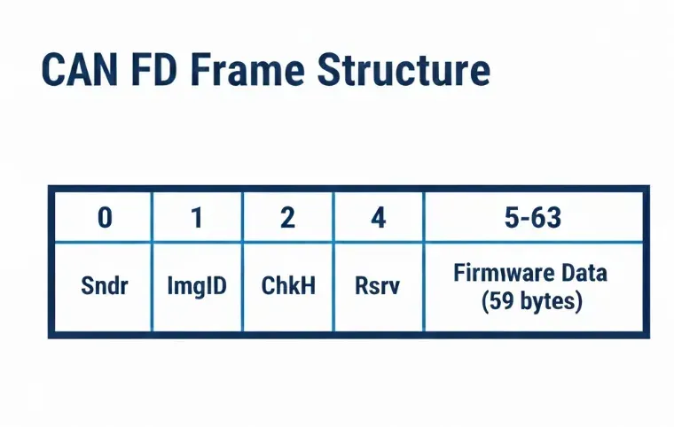
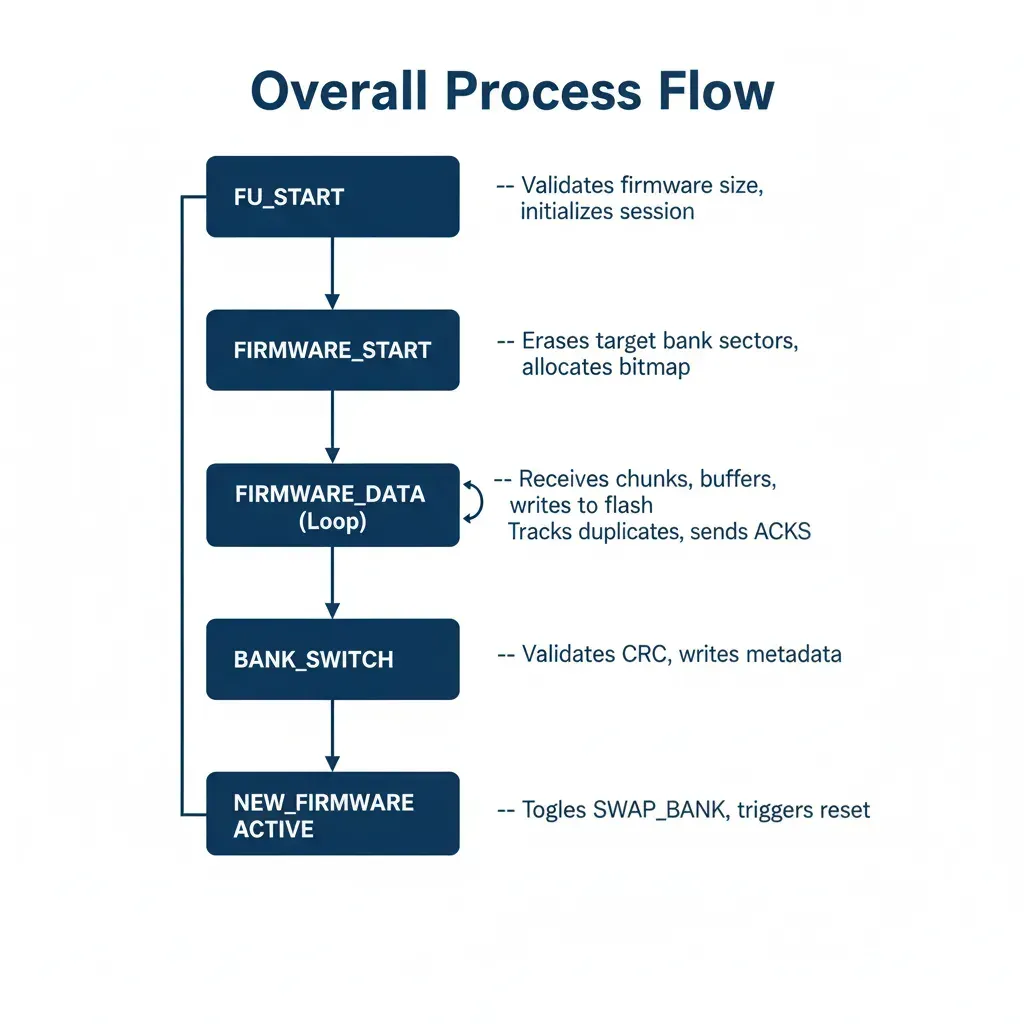
A CM4 host sends firmware via CAN FD (64-byte frames). The STM32H562 receives and buffers the data, performing flash writes in 16-byte aligned chunks into the target (inactive) bank. Validation confirms firmware integrity, and only then does the bank switch make the new firmware active.
This works because the active bank keeps running throughout the update, there's no downtime or broken intermediate state. If power is lost during the update, the old firmware is completely untouched and still works. If validation fails, the system simply stays on the old firmware.
Flash operations
Sector erase with bank awareness. You have to account for the current SWAP_BANK state before erasing, or you'll erase the wrong physical bank:
static error_t flash_erase_sector(uint32_t sector_addr, uint32_t bank_number) {
// CRITICAL: Determine physical bank based on current SWAP_BANK state
uint32_t optsr_cur = FLASH->OPTSR_CUR;
bool swap_bank = (optsr_cur & FLASH_OPTSR_SWAP_BANK_Msk) != 0;
uint32_t physical_bank;
if (swap_bank) {
// When swapped: Bank1 logical = Bank2 physical
physical_bank = (bank_number == 1) ? FLASH_BANK_2 : FLASH_BANK_1;
} else {
// Normal mapping
physical_bank = (bank_number == 1) ? FLASH_BANK_1 : FLASH_BANK_2;
}
uint32_t sector_offset = sector_addr & 0xFFFFF; // Offset within 1MB bank
uint32_t sector_num = sector_offset / SECTOR_SIZE;
FLASH_EraseInitTypeDef erase_init = {0};
erase_init.TypeErase = FLASH_TYPEERASE_SECTORS;
erase_init.Banks = physical_bank; // Use physical bank!
erase_init.Sector = sector_num;
erase_init.NbSectors = 1;
return HAL_FLASHEx_Erase(&erase_init, §or_error);
}Flash write with alignment. STM32H5 requires 16-byte (128-bit) aligned writes, and every write gets verified immediately after programming:
static error_t flash_write_data(uint32_t address, const uint8_t *data, uint32_t size) {
    if (size % 16 != 0 || address % 16 != 0) {
        return FU_ERROR_PARAM;
    }

    HAL_FLASH_Unlock();

    for (uint32_t i = 0; i < size; i += 16) {
        HAL_StatusTypeDef status = HAL_FLASH_Program(FLASH_TYPEPROGRAM_QUADWORD,
                                                    address + i,
                                                    (uint32_t)&data[i]);
        if (status != HAL_OK) {
            HAL_FLASH_Lock();
            return FU_ERROR_COMM_FAIL;
        }

        // Verify write
        if (memcmp((void*)(address + i), &data[i], 16) != 0) {
            HAL_FLASH_Lock();
            return FU_ERROR_COMM_FAIL;
        }
    }

    HAL_FLASH_Lock();
    return FU_OK;
}
Always pad your data to 16-byte boundaries, and never skip the alignment check.
Security considerations
Firmware validation runs multiple layers: magic number verification to reject invalid metadata, a CRC32 checksum for data integrity, reset vector validation to confirm valid firmware structure, and stack pointer validation to prevent overflow. Every check has to pass before new firmware is accepted.
Atomic updates come from the bank switching mechanism itself: it ensures atomic firmware replacement, gives rollback capability via a bank toggle on failure, and provides power-loss protection through the dual-bank architecture. If anything goes wrong mid-update, the system automatically stays on working firmware.
Communication security adds target node validation to prevent unauthorized updates, image ID tracking to prevent replay attacks, and timeout mechanisms to prevent resource exhaustion, so only the intended device accepts the update.
Best practices
Always check the SWAP_BANK state before erasing. Use 16-byte aligned writes throughout. Implement comprehensive validation before ever activating new firmware. Add watchdog protection during long operations. And test power-loss scenarios explicitly, don't just assume the architecture protects you.
Avoid forgetting to verify writes after programming, skipping CRC validation, ignoring alignment requirements, updating without proper testing, or overlooking timeout handling, each of these has caused real field issues for teams shipping similar systems.
Conclusion
The STM32H5's dual-bank architecture, combined with CAN FD optimization, gives a robust, production-ready firmware update solution: zero-downtime operation, power-loss safety, and automatic rollback. Field-deployed devices can be updated remotely with real confidence, knowing that even if something goes wrong, the system stays operational.
Technical specifications
Hardware: STM32H562 (ARM Cortex-M33 at 250 MHz), 2MB dual-bank flash, CAN FD capable. Software: FreeRTOS v10.x, HAL drivers (STM32CubeH5), custom CAN FD protocol.