
Placing EMI Filters Where They Actually Work on the PCB
Filter placement, return-path proximity, connector-side filtering, trace length control, and shield-boundary discipline
EMI problems are often discovered late.
The schematic looks correct. The filter components are selected from the datasheet recommendations. The simulation shows attenuation. The PCB passes functional testing. Then the product enters certification testing, and suddenly a few dB of margin disappear.
The common reaction is to search for a “stronger filter.”
A larger ferrite bead. A higher attenuation common-mode choke. More capacitors. Additional shielding.
But many EMI failures are not caused by the filter component itself.
They happen because the filter was placed where it cannot control the energy path.
A filter only works when the unwanted current is forced to pass through it. If noise can bypass the filter through a nearby return path, a connector shield, a ground gap, a long trace before the filter, or an uncontrolled cable exit, the component becomes almost irrelevant.
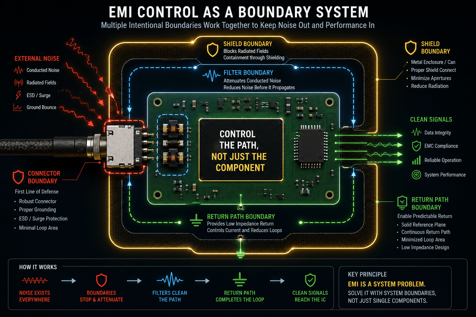
At Hoomanely, we look at EMI filters less as components and more as boundary-control elements.
The question is not:
“Did we add an EMI filter?”
The real question is:
“Did we place the filter at the point where noise tries to leave or enter the system?”
A good EMI design controls the path.
A poor EMI design only adds components.
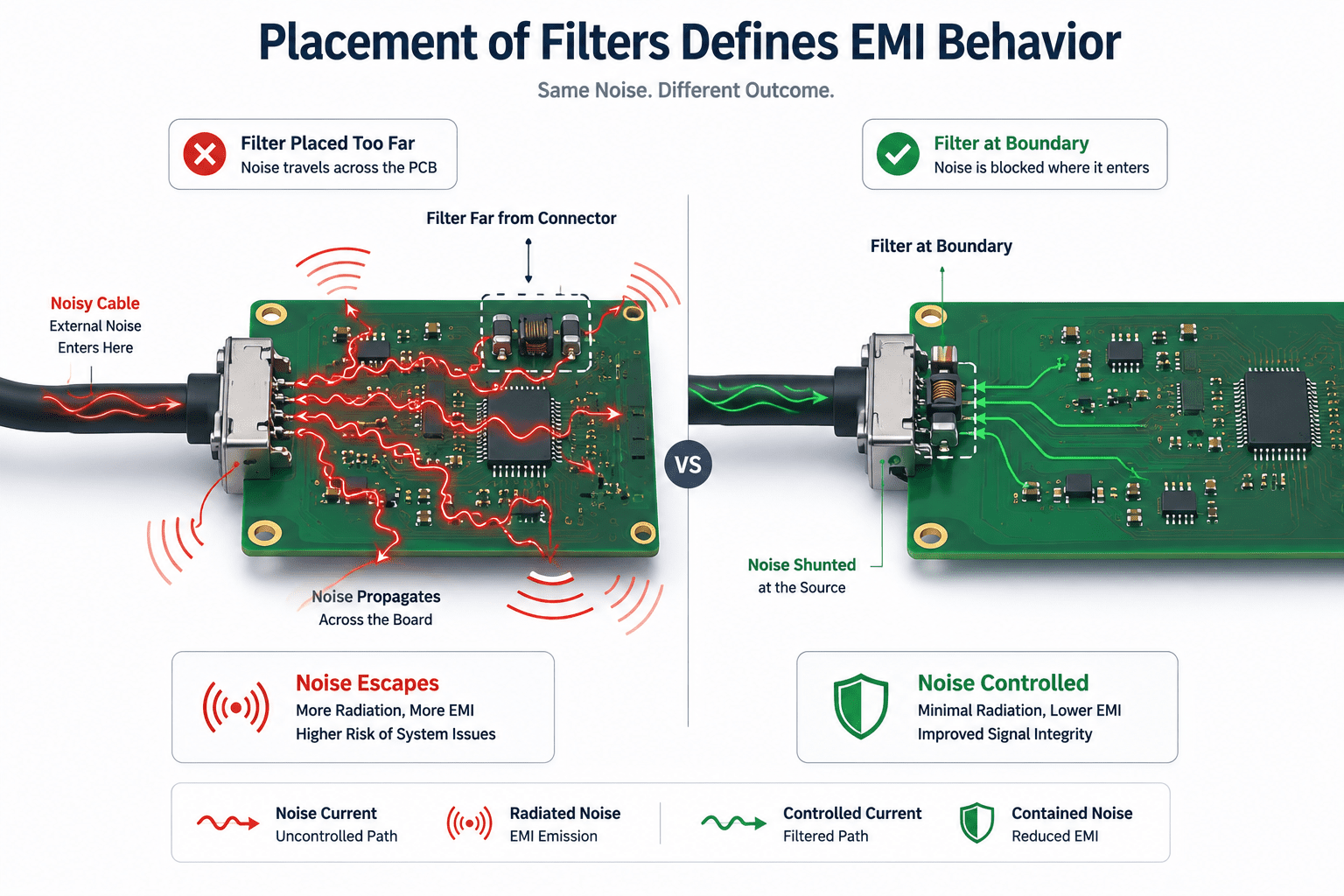
The Filter Location Is Part of the Filter Design
One of the easiest mistakes in PCB design is treating filter placement as a layout cleanup activity.
The schematic says:
Connector → Filter → IC
The PCB engineer places:
Connector → long trace → filter → long trace → IC
Electrically, the components exist.
Physically, the filter is no longer controlling the boundary.
High-frequency noise does not behave like a simple DC current moving through a wire. At higher frequencies, the PCB trace itself becomes part of the circuit. The distance between components, the return path underneath, the via placement, and the surrounding copper all influence the actual impedance.
A filter placed 30 mm away from a connector is not filtering the connector boundary.
It is filtering a point somewhere inside the product.
By the time the signal reaches the filter, the noise current may already have coupled into:
- chassis structures,
- cable shields,
- neighbouring traces,
- ground planes,
- connector pins.
The filter may still reduce conducted noise internally, but it has already lost control of the emission path.
For external interfaces, the filter location should usually be decided first, before routing begins.
The connector is where the outside world enters.
That is where the noise boundary exists.
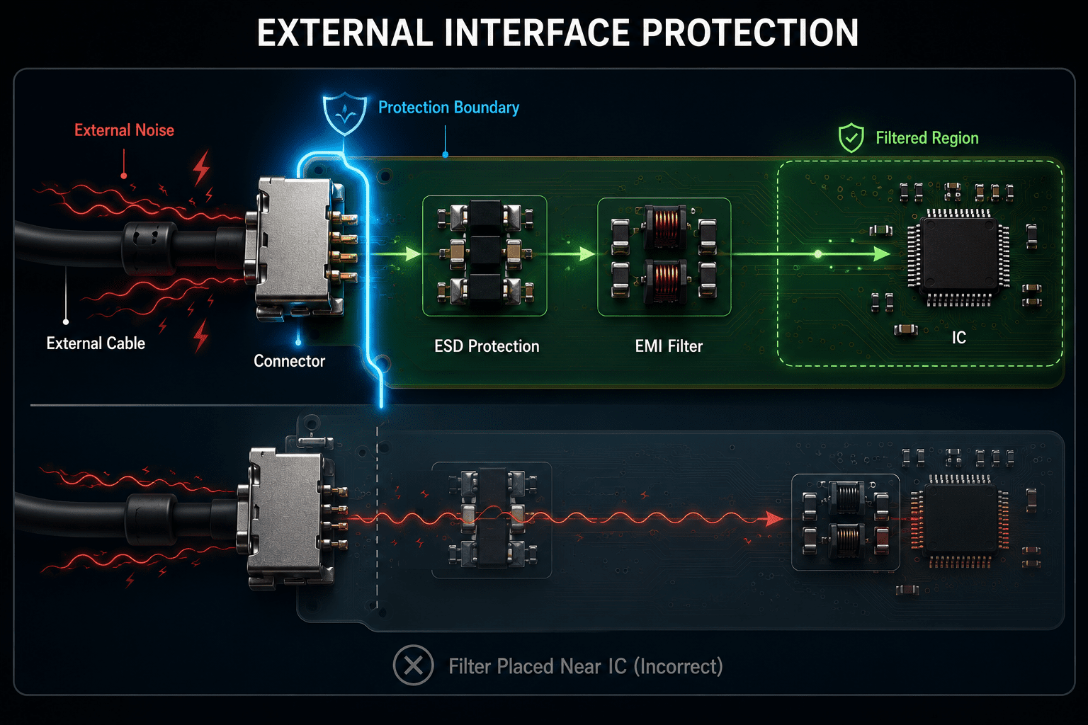
Connector-Side Filtering Protects the Real Entry Point
External connectors are one of the most common EMI escape paths.
USB, Ethernet, display interfaces, power inputs, sensor cables, and communication connectors all create a direct electrical connection between the PCB and the outside environment.
The cable is often the antenna.
The connector is often the coupling point.
If the filter is placed close to the IC instead of the connector, the noisy section of the PCB remains exposed.
A practical layout approach is:
Connector → Protection → Filter → Clean PCB Region → IC
The area between the connector and filter should be treated as an exposed zone. It should be short, controlled, and isolated from sensitive circuits.
For example, on a communication interface:
A common-mode choke placed near the transceiver may still reduce noise. But placing it directly near the connector provides better control because the common-mode current is stopped before it enters the larger PCB area.
The same applies to power inputs.
A TVS diode, fuse, common-mode choke, and filtering capacitor network should usually sit close to the entry point. Otherwise, transient and high-frequency energy travels through the board before being controlled.
The filter should protect the board from the connector.
Not protect the connector from the board.
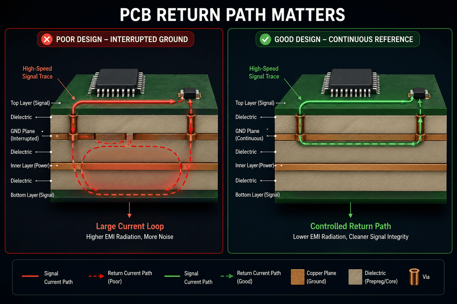
Return Path Proximity Decides Whether Filtering Works
Many EMI issues come from looking only at signal traces.
The return path is equally important.
A signal current always needs a return path. At high frequency, that return current follows the path of lowest impedance, usually directly underneath the signal trace on the reference plane.
When a filter component is placed in the signal path but the return path is not controlled, the noise simply finds another route.
Consider a connector filter:
A signal passes through a common-mode choke.
But the connector shield connects to chassis through a long narrow trace.
Or the filter capacitor returns to ground through a long via path.
Or the reference plane is interrupted underneath the filtered section.
The intended filtering path has higher impedance than the unintended path.
The noise chooses the easier route.
At Hoomanely, return-path discipline is considered part of the filter placement itself.
For every EMI component, we ask:
Where does the high-frequency current return?
How long is that path?
Does it cross a plane split?
Does it enter the sensitive PCB area before reaching ground?
A filter without a controlled return path is only half a filter.
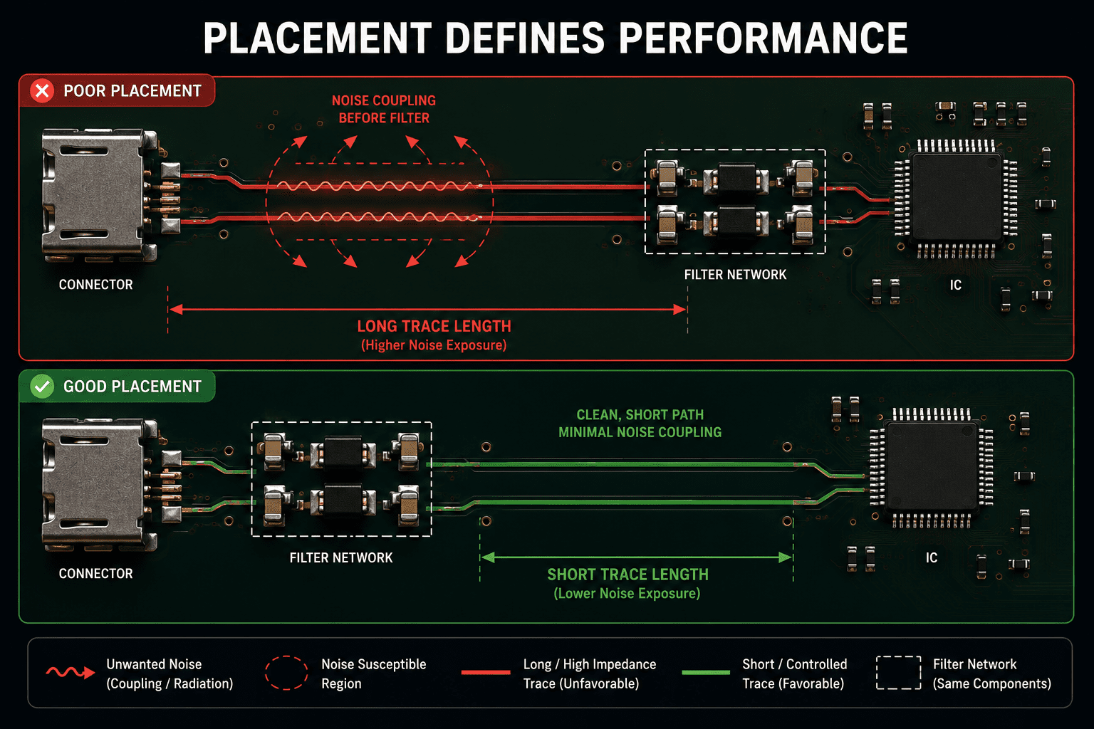
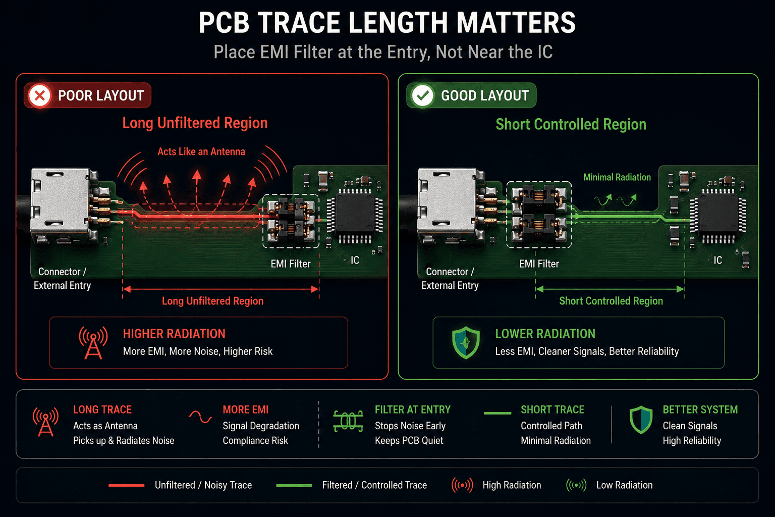
Trace Length Before Filtering Is an EMI Decision
Before-filter trace length is often underestimated.
Engineers usually focus on the component values:
“Should we use 100 pF or 1 nF?”
But the trace before that capacitor or ferrite may determine whether either value matters.
A long unfiltered trace behaves like an antenna.
A connector pin carrying a noisy signal travels several centimeters across the PCB before reaching the filter. During this distance, the energy can already radiate or couple into neighbouring circuits.
The filter might reduce the noise after that point, but it cannot remove the energy that already escaped.
The best practice is simple:
Keep the unfiltered region physically small.
This means:
- Place filter components immediately after connectors.
- Avoid routing noisy signals through clean PCB areas before filtering.
- Keep filter-to-connector connections short and direct.
- Avoid unnecessary vias before the filter.
- Maintain continuous reference planes underneath the path.
In high-speed interfaces, this becomes even more important because the edge rate creates high-frequency content far beyond the nominal data frequency.
A 100 MHz signal with a fast edge can contain several GHz of energy.
The filter placement must consider the edge, not only the clock.
Shield Boundaries Must Be Designed, Not Added Later
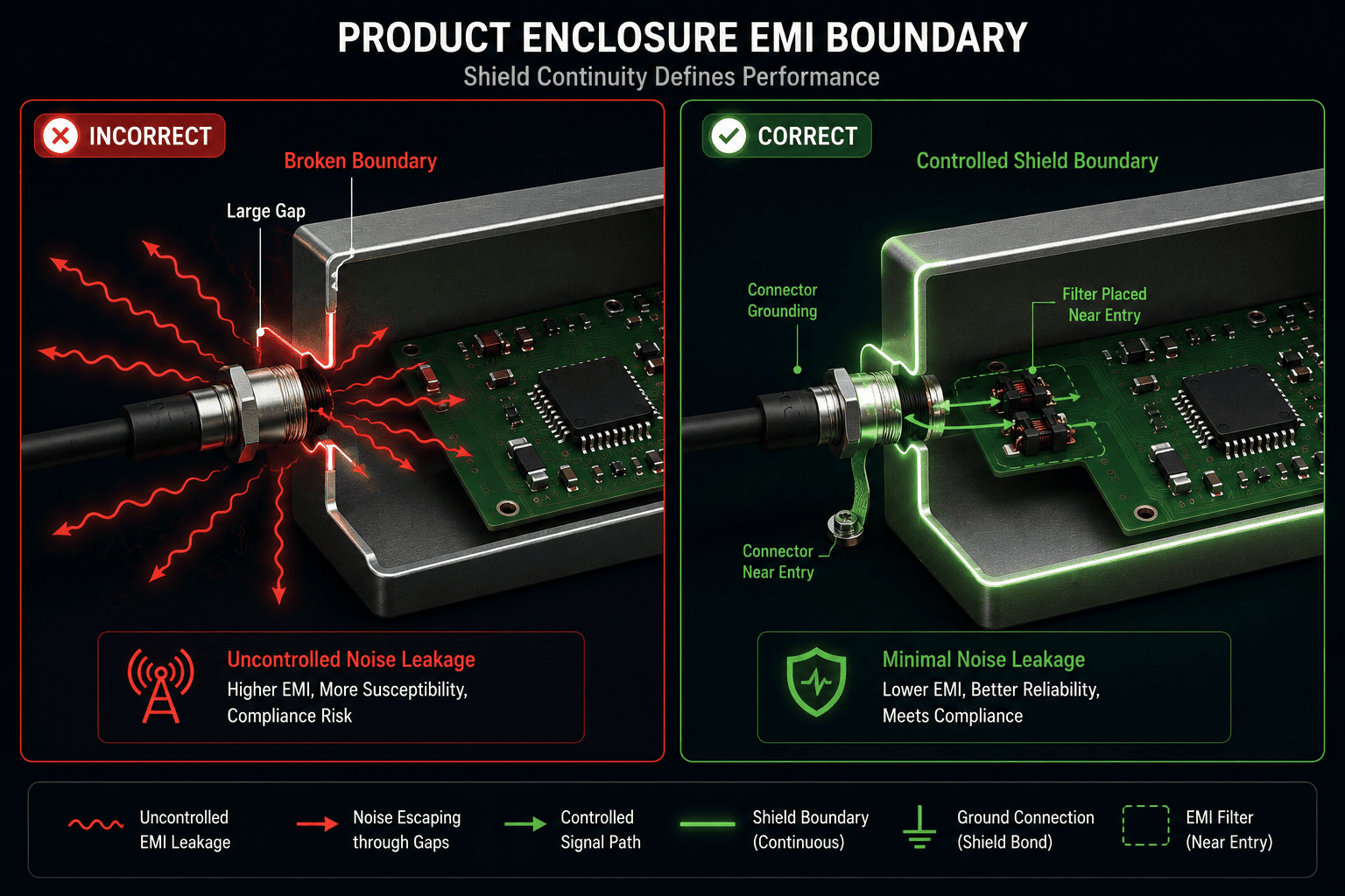
A shield enclosure does not automatically solve EMI.
A shield works only when the boundary is electrically continuous.
Many products fail because the PCB filtering and enclosure shielding are designed separately.
The connector exits through the enclosure.
The cable shield connects somewhere else.
The PCB ground connects at another location.
Now there are multiple uncontrolled paths around the boundary.
The noise current does not know where the designer intended the shield boundary to be.
It simply follows the available impedance.
A good architecture defines one clear transition:
External environment → Shield boundary → Filtered PCB region
The filter should sit close to this transition.
For connector interfaces, this often means:
- short connection between connector shield and chassis reference,
- controlled ground stitching around connector areas,
- filtering before signals enter the main PCB area,
- avoiding large openings in the shield near noisy circuits.
The goal is not only reducing noise.
The goal is preventing noise from entering the product environment.
Do Not Mix Protection and Filtering Without Understanding Their Roles
Another common PCB mistake is placing all protection components together without understanding their function.
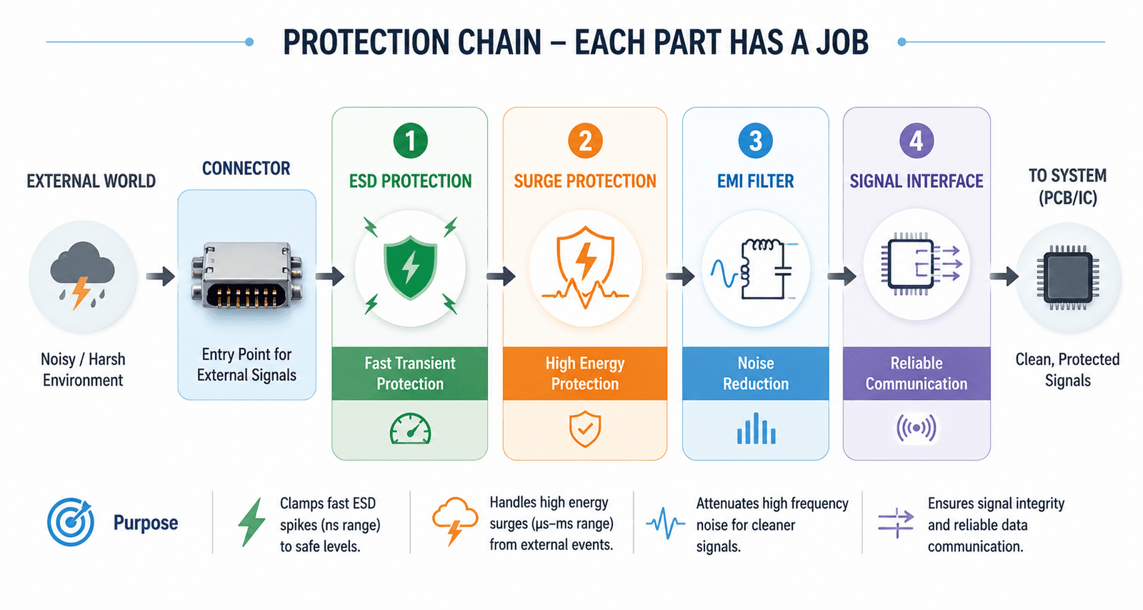
ESD protection, surge protection, EMI filtering, and signal conditioning solve different problems.
An ESD diode protects against very fast high-voltage events.
A common-mode choke reduces common-mode noise.
A capacitor provides high-frequency shunting.
A ferrite bead blocks high-frequency energy.
Their placement should follow their purpose.
For example:
An ESD device should be extremely close to the connector because the transient energy must be diverted before entering the PCB.
A filter may follow after it.
Placing the ESD device near the IC because “there was more space” can allow the transient energy to travel through the board first.
Similarly, placing filtering components far away from the connector because the schematic looks cleaner usually creates an uncontrolled noisy region.
Good EMI design starts by understanding current flow during the unwanted event.
Filter Placement Should Support Debugging Too
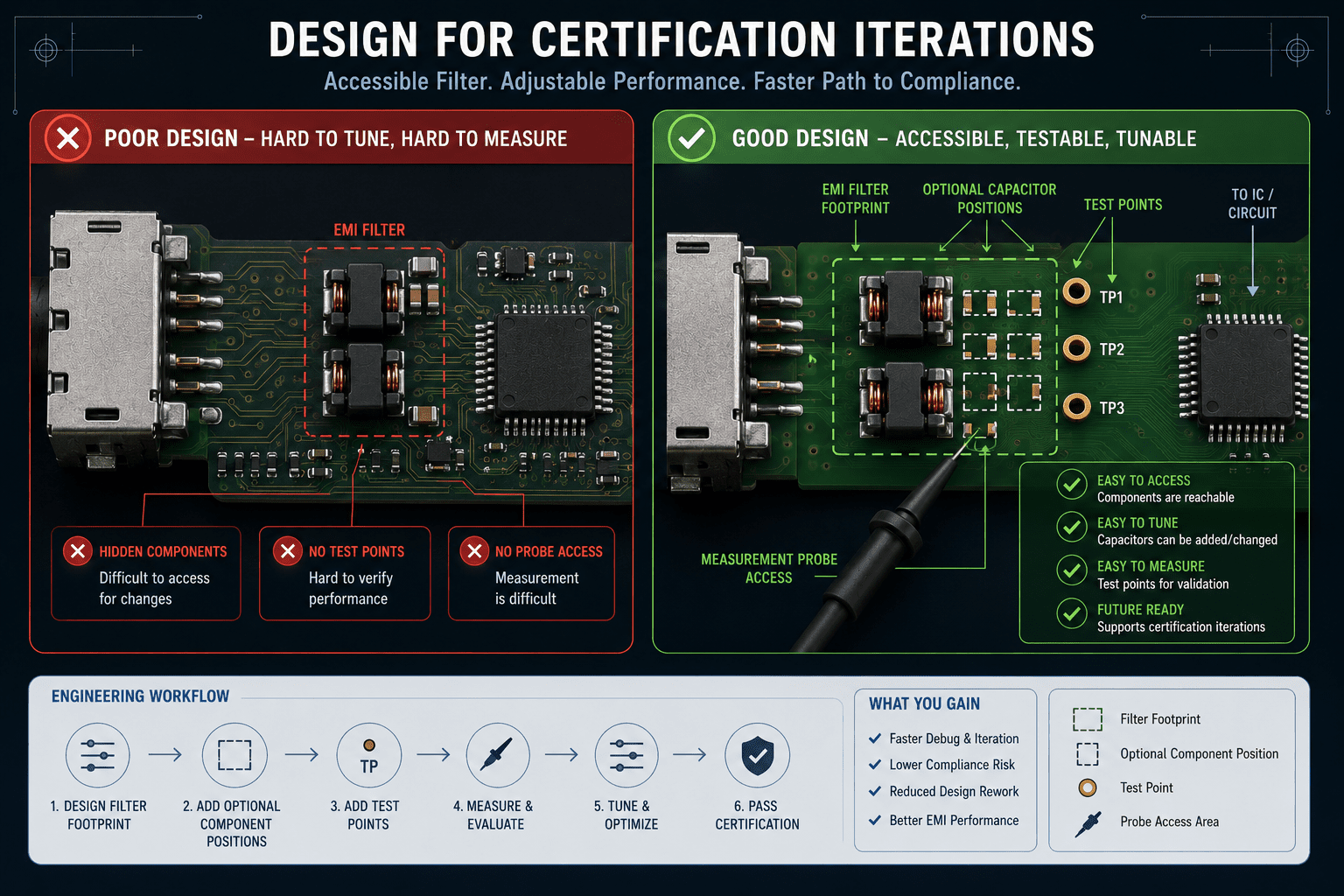
EMI fixes are often iterative.
During certification, engineers may need to modify capacitor values, change ferrite characteristics, or add common-mode filtering.
A good PCB architecture makes these changes possible.
Poor placement makes EMI tuning painful.
Useful practices include:
- keeping filter footprints accessible,
- providing optional component locations,
- avoiding buried filtering networks,
- adding measurement points near interfaces,
- keeping noisy and quiet zones visually separated.
The PCB should tell the engineer where the noise boundary exists.
A board where filters are scattered randomly becomes difficult to debug because nobody knows which region is supposed to be controlled.
Intent preservation matters.
Future engineers should understand why a filter exists.
Not just that it exists.
Hoomanely View: EMI Filters Are Boundary Tools, Not Magic Components
At Hoomanely, EMI filtering is treated as an architecture decision.
The component value matters.
The ferrite impedance matters.
The capacitor selection matters.
But the physical placement determines whether those components are actually controlling the current path.
A filter placed at the wrong location becomes decoration.
A filter placed at the correct boundary becomes protection.
The strongest EMI designs are not the ones with the most filters.
They are the ones where every filter has a clear responsibility:
This filter controls this connector.
This capacitor closes this return path.
This choke prevents this cable from becoming an antenna.
This shield boundary stops this current from entering the wrong region.
Final Thoughts
EMI problems rarely come from missing components.
They usually come from uncontrolled paths.
A PCB can have excellent filter parts and still fail because the noise never reaches the filter. The return path was ignored. The connector boundary was uncontrolled. The trace before filtering was too long. The shield transition was incomplete.
Good EMI design is about controlling where current flows.
Place filters where the noise enters.
Keep return paths close.
Control the boundary.
Minimize unfiltered distance.
Respect the physical structure of the PCB.
Because in real hardware, the filter does not work because it is on the schematic.
It works because the PCB gives it the only path available.