Surviving Silent Silicon: Cache, ECC, and Self-Healing NMI Handlers

A double-bit error in the application flash of a deployed device is not a
theoretical event. It is what happens when a stray neutron — or simply an aging
storage cell — flips two bits in a single sixteen-byte ECC word at the wrong
instant, in the wrong region, on a customer's living-room shelf. Without a
firmware response, the next instruction fetch from that address dumps the
device into a fault loop with no log, no telemetry, and no path back. At
Hoomanely, the camera node that anchors our pet monitoring system is built so
that this failure mode never reaches the customer. The non-maskable interrupt
handler decodes the ECC fault register, identifies the failing eight-kilobyte
sector, distinguishes bootloader memory from application memory, and self-erases
the failing sector before the device is ever rebooted. Building that handler —
and the cache, RAM ECC, and memory-protection configuration that surrounds it —
is what this post is about.
The Problem: Speed and Integrity at 250 MHz
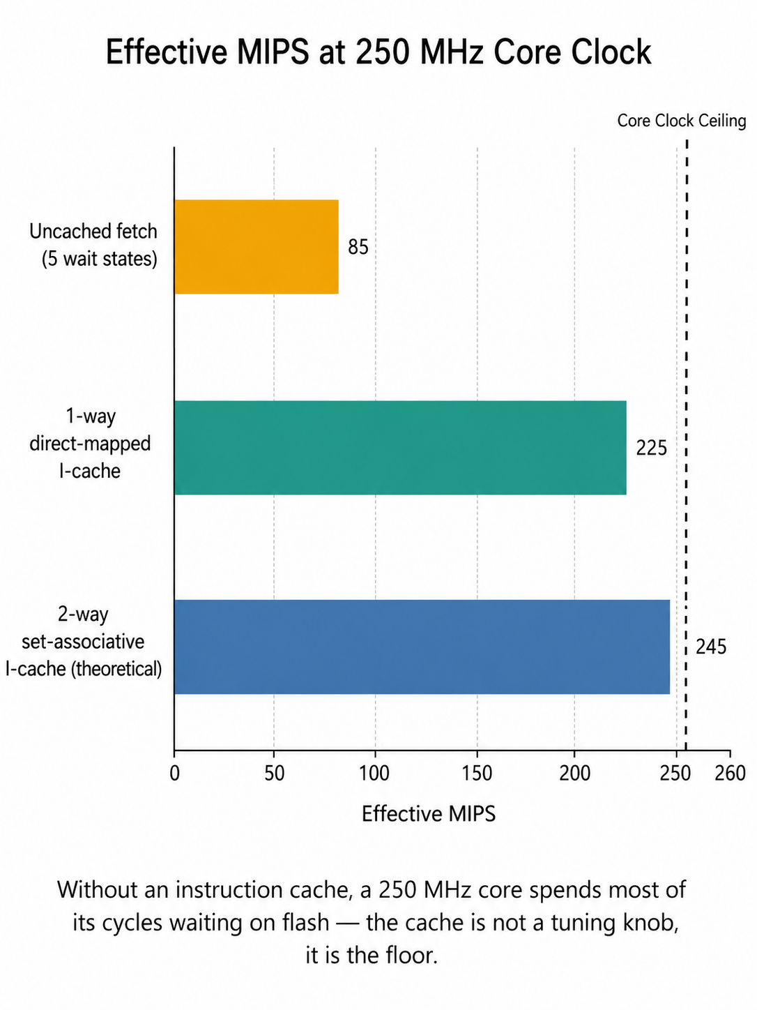
When an application core runs at 250 MHz from on-chip flash, two physical
realities collide. The flash array cannot return a 32-bit instruction word in a
single 4 ns clock period — five wait states are typical at this speed. Without
an instruction cache between the core and the flash interface, the CPU spends
most of its life stalled, and a 250 MHz core delivers something closer to
80–100 MHz of useful work. The first job of the memory subsystem is therefore
acceleration.
The second job is integrity. The same density that lets us fit megabytes of
application code on a single die makes that code increasingly susceptible to
single-event upsets — bit-flips driven by cosmic background radiation or by
slow cell drift over years of deployment. Single-bit flips can be silently
corrected by the flash controller's ECC. Double-bit flips cannot — and an
uncorrected double-bit flip in code memory is the definition of a fault that
the running CPU cannot recover from on its own.
Both problems sit one layer below every algorithm in our firmware. They are
not optimisations; they are preconditions.
The Approach: A Direct-Mapped Instruction Cache
The instruction-cache initialisation in our firmware is short and intentional:
/* Enable instruction cache in 1-way (direct mapped cache) */
if (HAL_ICACHE_ConfigAssociativityMode(ICACHE_1WAY) != HAL_OK) {
    Error_Handler();
}
if (HAL_ICACHE_Enable() != HAL_OK) {
    Error_Handler();
}
The non-default choice is the 1-way direct-mapped mode. In a direct-mapped
cache, every instruction address maps to exactly one cache line — there is no
associativity search at lookup time. The benefit is lower lookup energy and
simpler, more predictable timing; the cost is that two hot functions whose
addresses happen to share an index will conflict and evict each other. For a
small, statically linked firmware where the call graph is well understood, that
trade is a win, especially when the target is a battery-aware device living on
a customer's shelf for months at a time.
A second detail worth noting: associativity must be configured before the
cache is enabled. The hardware does not allow re-configuration of an active
cache; calling these two HAL routines in the wrong order yields an enabled
cache locked into whatever the reset value happened to define.
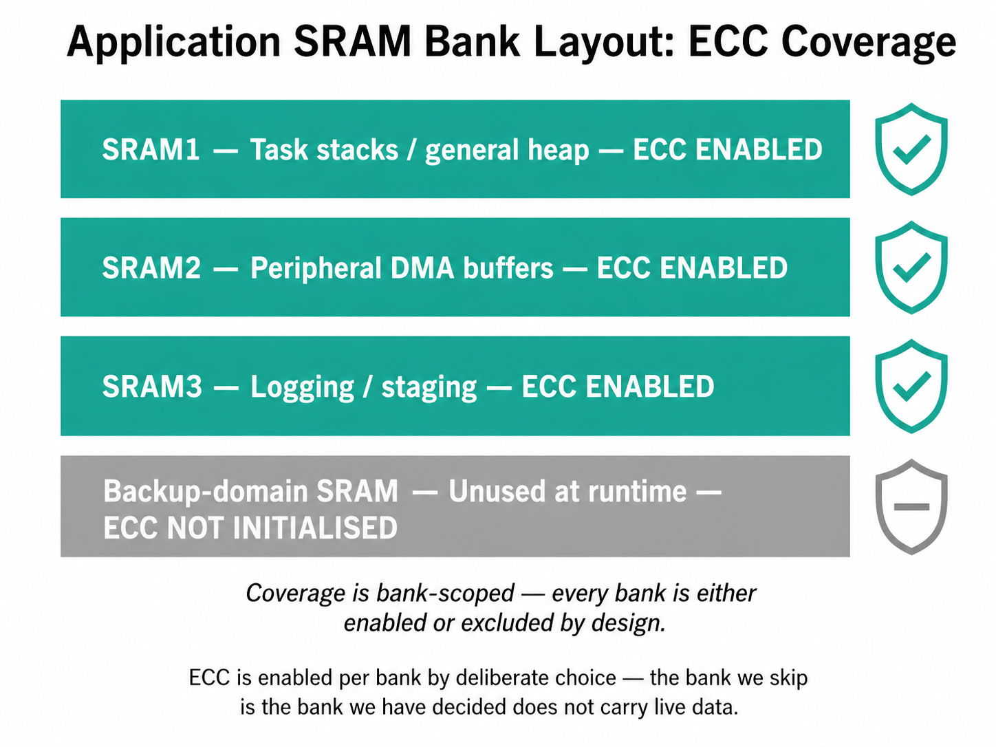
The Approach: ECC on the Banks That Carry Live Data
Application SRAM on our MCU is split across multiple physical banks. Three of
those banks hold live application data — task stacks, heap regions, peripheral
DMA buffers — and each one is brought up under explicit RAMCFG configuration:
hramcfg_SRAM1.Instance = RAMCFG_SRAM1;
HAL_RAMCFG_Init(&hramcfg_SRAM1);
hramcfg_SRAM2.Instance = RAMCFG_SRAM2;
HAL_RAMCFG_Init(&hramcfg_SRAM2);
hramcfg_SRAM3.Instance = RAMCFG_SRAM3;
HAL_RAMCFG_Init(&hramcfg_SRAM3);
HAL_RAMCFG_Init does two things at the register level: it gates the RAMCFG
peripheral clock on for the bank and it activates the bank's ECC machinery.
The peripheral clock is the dependency that catches most teams out — without__HAL_RCC_RAMCFG_CLK_ENABLE(), every subsequent RAMCFG write is a silent
no-op and ECC errors go undetected.
A fourth backup-domain SRAM bank exists on the part but is not used by the
application path, so it is deliberately omitted from this initialisation. The
principle is simple: enable ECC on every bank that holds data the device's
behaviour depends on, and skip the banks that do not. Every bank that escapes
the loop is a bank where a silent flip can corrupt a frame, a sensor reading,
or a control variable without any signal at all.
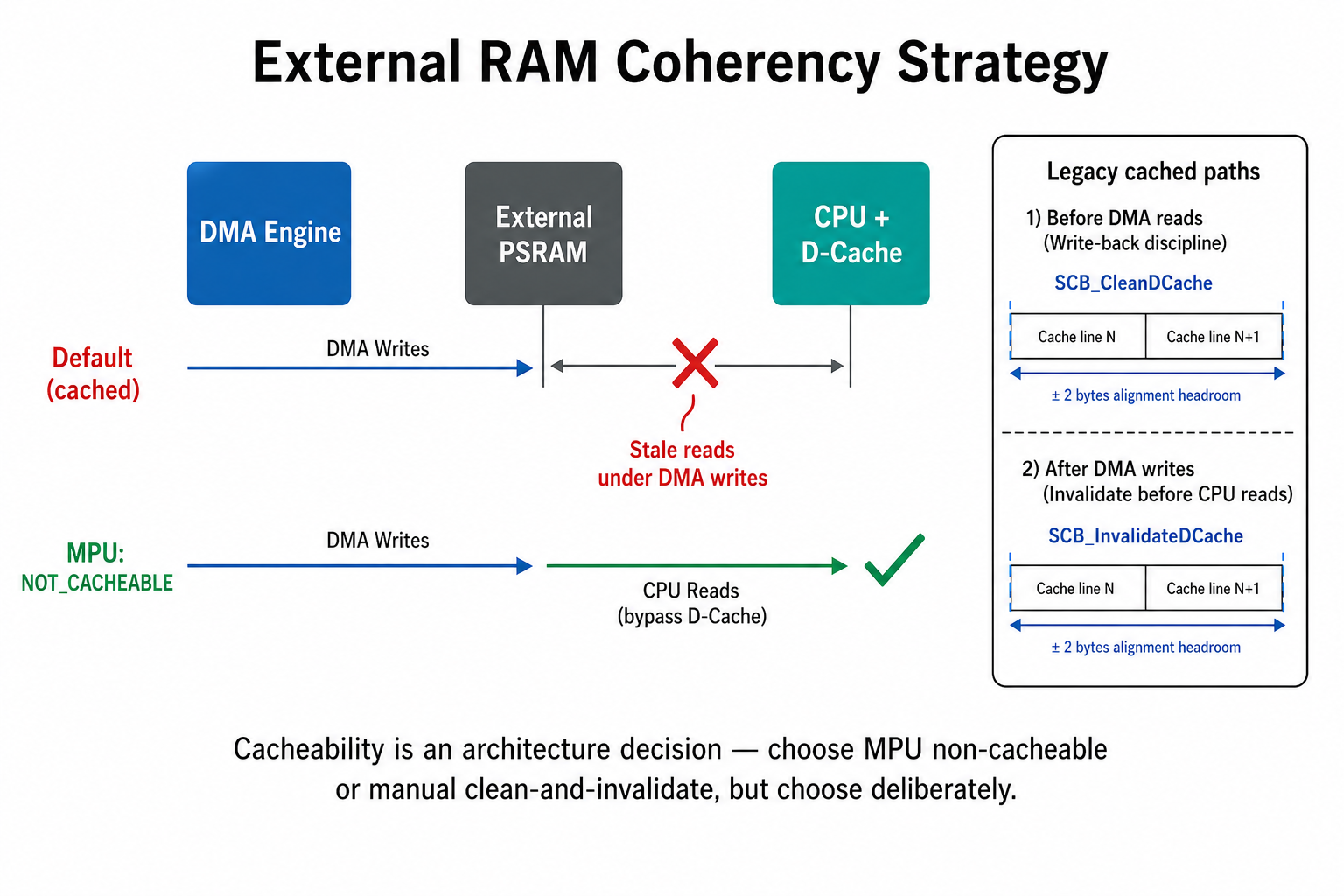
The Approach: External RAM Without the Cache, On Purpose
Our diagnostic capture pipeline lands raw frames in an external PSRAM tier
before they are compressed and transmitted. DMA writes those frames in; the
CPU reads them out for compression. The naive configuration — letting the data
cache cache PSRAM accesses — produces a coherency bug where DMA writes go to
physical PSRAM but the CPU reads stale cached copies.
We resolved this at the memory-protection layer rather than in software:
/* Define cacheable memory via MPU - Configure PSRAM as Device-nGnRnE */
attr.Attributes = INNER_OUTER(MPU_NOT_CACHEABLE);  /* Normal memory, but no
                                                       cache to prevent DMA
                                                       coherency issues */
For the few legacy code paths that still flow through cached regions, manual
cache discipline applies. The pattern in our PSRAM utility layer carries a
comment that comes from a real bug, not a textbook:
/* CRITICAL FIX: Clean cache starting 2 bytes BEFORE the write address
   to clear any stale cache data that might overlap the boundary. */
SCB_CleanDCache_by_Addr((uint32_t *)clean_start, (int32_t)clean_size);
The lesson the comment encodes is alignment headroom. ASCB_CleanDCache_by_Addr call that starts exactly at the write address can
leave bytes of a partially-cached preceding line in stale state, because cache
lines are wider than the byte the caller cares about. Backing the clean range
up by a couple of bytes — and rounding the size up to a cache-line multiple —
is the difference between a write that survives and a write that does not.
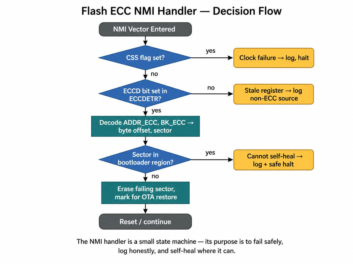
The Process: A Self-Healing NMI Handler for Flash ECC
The most consequential piece of the memory subsystem is the non-maskable
interrupt handler that fires on a flash double-bit error. A double-bit flip in
code memory means the next instruction fetch from that address returns garbage;
the CPU cannot reliably continue executing. The NMI fires before the
conventional fault handlers do, giving firmware exactly one chance to respond.
The first job in the handler is to decode the failure:
uint32_t eccdetr   = FLASH->ECCDETR;
uint32_t addr_ecc  = eccdetr & 0x0000FFFFUL;
uint32_t bk_ecc    = (eccdetr >> 22U) & 0x1U;
uint32_t byte_off  = addr_ecc * 16UL;        /* 16-byte ECC word granularity */
uint32_t bank_base = bk_ecc ? 0x08100000UL : 0x08000000UL;
The ADDR_ECC field gives the index of the failing 16-byte ECC word inside
the bank; the BK_ECC bit identifies which bank; the ECCD flag at bit 31
confirms a double-detection event actually occurred.
The second job is disambiguation. Several different conditions can raise
the NMI line, including a clock-security failure, and the ECCDETR register
may simply hold stale data from an earlier event. Before acting, the handler
validates the source:
if (!(eccdetr & 0x80000000UL)) {
    /* Not an ECC source — likely a clock-security or other NMI */
}
The third job is to log the failure through the most primitive transport the
firmware has — direct polled UART, no DMA, no RTOS calls. If flash is
corrupt, the descriptor tables driving DMA may be too, and any abstraction
layer above the bare register interface is a risk in a moment when the device
is already in a half-trustworthy state.
The fourth job is recovery. The handler classifies the failing sector against
the bootloader region and erases it only when it is safely re-erasable:
bool is_bootloader = (bk_ecc == 0U && sector_in_bk < 4U);
if (!is_bootloader) {
    erase.Banks  = bk_ecc ? FLASH_BANK_2 : FLASH_BANK_1;
    /* erase the failing sector — application content can be restored
       on next boot from the recovery partition */
}
A bit-flip in a bootloader sector is unrecoverable in flight — erasing it
would destroy the device's only known-good entry point. Application sectors,
by contrast, are erasable: the content is lost, but a clean sector can be
rewritten from the recovery image at the next boot, and the device stays alive
in the meantime.
The Process: Init Order Matters
The boot sequence is not arbitrary. The order in our firmware is:
- Core HAL initialisation — system control block, basic peripherals.
- System clock configuration to the target 250 MHz.
- RAMCFG bring-up — SRAM ECC active before any heap allocation occurs.
- Instruction cache enable — code now runs at full speed.
- Memory protection unit configured — external PSRAM marked non-cacheable.
- Application initialisation — peripherals, RTOS, tasks.
The principle is that every layer of memory protection must be in place before
the workload that depends on it begins. Enabling the cache before clocking
RAMCFG would mean a window during which application data lives in SRAM that is
not yet ECC-monitored — and a flip in that window is invisible afterwards.
Why It Matters at Hoomanely
Hoomanely's mission is to reinvent pet healthcare through Physical
Intelligence — continuous, AI-powered monitoring that gives owners and
veterinarians clinical-grade insight into a pet's wellbeing before symptoms
become visible. The camera node at the heart of that system runs an
imaging-and-thermal pipeline that captures, compresses, and transmits
diagnostic frames to the Biosense AI Engine for analysis.
Three things in this post hold that pipeline up. The instruction cache is what
lets compression and image-processing code execute at the cadence the camera
demands; without it, frame budgets collapse and the capture loop falls behind
the sensor. The SRAM ECC is what lets the AI engine trust that a thermal value
or a frame buffer reaching the network is the same one the sensor produced.
The flash NMI handler is what ensures that a single bit-flip in a customer's
home — at any hour, in any deployment, with no engineer in the loop — does not
silently end that pet's monitoring stream.
The throughline is straightforward. Speed, integrity, and survivability are
not three separate problems — they are the same problem at three layers of the
silicon.
Key Takeaways
- The instruction cache is a floor, not a knob. At 250 MHz a flash-bound
core without I-cache delivers a fraction of its rated performance — picking
associativity intentionally is part of the design, not an afterthought. - ECC is per-bank, and the bank you skip is the bank that can lie to you.
Enable RAMCFG on every memory region that carries live application data;
treat any skip as a deliberate, documented decision. - External RAM cacheability is an architecture choice. Either mark the
region non-cacheable in the memory protection unit, or commit to manual
cache discipline at every DMA boundary. The middle ground is silent
corruption. - Cache clean and invalidate must include alignment headroom. Cache lines
are wider than the bytes you care about; back the range up and round the
size up, or the next read will surprise you. - A flash ECC NMI handler is the difference between self-healing and
bricking. Decode the fault register, log through the most primitive
channel you trust, classify by bank and sector, and only erase what is
safely re-erasable.
At Hoomanely, the imaging-and-thermal pipeline runs at 250 MHz because the
cache makes that achievable, the AI engine trusts the data because ECC makes
the SRAM honest, and the device survives long enough to do both because the
NMI handler refuses to let a single bit-flip become a brick. None of these
mechanisms are visible to a pet owner, and that is the point — preventive care
depends on a sensor stream the owner never has to think about. Physical
Intelligence starts with getting the silicon to behave, and stays trustworthy
by refusing to look away when it does not.