The Anatomy of vBus: Understanding Connector Pin Blocks
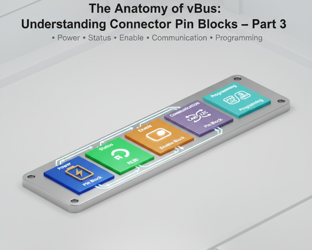
We've talked about 100-pin CPU SoMs, 30-pin Power SoMs, and the challenges of standardization. But here's a question worth answering directly: what exactly lives on those pins? A connector with 40, 50, or 100 pins can quickly become overwhelming chaos without a clear organizational strategy. This is why we've adopted a rigorous pin-block architecture for vBus, five fundamental blocks that form the foundation of every connector:
- Power
- Status
- Enable
- Communication
- Programming
Power block: the foundation
The Power Block is intentionally kept simple and pure, it delivers electrical energy, period, no control signals, no mixed functions. Our standard block includes three voltage rails chosen from extensive analysis of common embedded requirements. The 5V rail is the workhorse for many peripherals, sensors, and legacy components, with multiple pins (2-4 depending on connector size) reducing resistance and distributing thermal stress. The 3.3V rail is the de facto standard for modern digital logic and communication interfaces like I2C, SPI, and UART, powering the majority of digital components. The 1.8V rail serves high-performance processors, MIPI interfaces, DDR memory, and modern low-power components.
Ground pins are just as important as power pins, arguably more so. A poor ground connection causes voltage offsets between modules leading to communication errors, ground bounce during high-speed switching that corrupts data signals, EMI and noise coupling, and measurement errors in analog circuits. We allocate a generous number of ground pins, often equaling or exceeding the combined positive voltage pins, and in high-speed designs we strategically place ground pins adjacent to differential pairs for clean return paths.
We deliberately exclude power-good signals, enable controls, and voltage monitoring from this block, those belong elsewhere. This separation gives clarity (anyone looking at the schematic immediately knows the block contains only passive power delivery), isolation (keeping noisy switching signals away from power delivery paths reduces interference), and modularity (the same power pin assignments work across different SoM types regardless of control architecture). The Power Block is designed to be the most stable, most boring part of the connector, and that's exactly what we want.
Status block: visual intelligence
The Status Block uses a deceptively simple concept, a single RGB LED per SoM, specifically a WS2812 or similar addressable LED. It needs only one GPIO pin via a serial protocol, offers a full color spectrum for encoding complex state information, and is chainable so multiple LEDs can be daisy-chained on the same data line.
Our standard color encoding maps system states clearly: solid green for normal operation, solid blue for programming mode, solid yellow or amber for a warning state, solid red for a critical error, pulsing green for boot in progress, pulsing blue for active communication, flashing red for a critical fault, magenta for debug mode, white for factory test, off for powered down or sleep. Beyond basic states, pulse frequency can indicate data throughput, color cycling can show progress through a multi-step process, brief flashes can acknowledge commands, alternating colors can indicate conflict.
Imagine debugging a system with five SoMs, at a glance you see the CPU SoM pulsing green (running normally), the Power SoM solid green (stable), two Peripheral SoMs pulsing blue (streaming data), and a Communication SoM flashing yellow-blue (attempting to connect). You instantly understand system state without connecting a debugger. The CPU SoM can even orchestrate synchronized patterns across modules, a successful cloud upload might trigger a green wave cascading across all SoMs. The Status Block typically occupies just 1-2 pins but the information density it provides is remarkable.
Enable block: intelligent power management
The Enable Block introduces selective module control, the ability to dynamically enable, disable, or reset individual modules for power management, fault isolation, and system optimization. Each Peripheral SoM has a dedicated enable signal controlled by the CPU SoM. For power optimization, in battery-powered applications you don't always need every sensor active, we've seen systems reduce average power consumption 40-60% through intelligent enable management. For fault isolation, if a Peripheral SoM enters a fault state and starts drawing excessive current or flooding the bus, the CPU can detect it through current monitoring or communication timeouts and disable the offending module without affecting the rest of the system.
The Enable Block also enables controlled hot-swap and reset, disable the module, stabilize power and communication, re-enable with proper timing, then initialize the newly started module, especially important for modules with complex startup sequences. Implementation typically uses dedicated enable pins gating power regulators or reset circuits via a load switch or MOSFET, sometimes with soft-start circuits to prevent inrush spikes.
In complex systems, modules have power-up dependencies, the Power SoM must be stable before enabling other modules, the CPU SoM must boot before enabling Peripheral SoMs, certain sensors need a specific warm-up sequence. The Enable Block combined with software control allows sophisticated sequencing. Many SoMs also include watchdog circuits monitoring the enable line, if the CPU SoM becomes unresponsive and stops toggling watchdog signals, a hardware watchdog can pull enable lines low, forcing a system-wide reset, a failsafe recovery mechanism even when software has completely failed.
Communication block: the data highway
At the core of the Communication Block is FDCAN, the flexible data-rate version of CAN. This might seem unconventional compared to USB or Ethernet, but for good reasons. Robustness, CAN was designed for harsh automotive and industrial environments with extensive error detection, automatic retransmission, and fault confinement. Multi-master architecture, unlike master-slave SPI or point-to-point UART, any node can initiate communication without complex arbitration logic. Priority-based arbitration, non-destructive bitwise arbitration lets higher-priority messages win bus access without collisions or delays. Speed, CAN FD allows up to 8 Mbps in the data phase, more than adequate for many sensor applications, achieved with simple twisted-pair wiring. And distance and reliability, CAN maintains signal integrity over several meters, far better than high-speed serial protocols requiring careful impedance matching. We allocate two pins for FDCAN, CANH and CANL, with an optional third for dynamic termination control.
Alongside FDCAN, we include a dedicated I2C interface serving a different purpose. Module identification lets each SoM store type, capabilities, serial number, calibration data, and firmware version in an onboard EEPROM, enumerable similar to USB device enumeration. Configuration and control leverages the I2C-based configuration registers most sensors already support, rather than creating custom protocols over FDCAN. Low-speed communication for infrequent transactions like reading module temperature is simpler and more power-efficient than spinning up FDCAN messages. And I2C natively supports up to 127 devices with built-in addressing, perfect for systems with many simple modules.
The third element is an interrupt pin. Polling is inefficient, constantly asking each Peripheral SoM "do you have data" wastes processor cycles and power. Instead, Peripheral SoMs assert an interrupt line when they have important data, enabling event-driven architectures, a motion sensor triggers an interrupt on movement, a communication module interrupts when data arrives, a fault condition immediately signals the CPU. The interrupt pin is typically open-drain, allowing multiple modules to share the same line in a wired-OR configuration, with the CPU servicing the interrupt and querying via I2C to determine the source. In summary, the Communication Block typically occupies 5-6 pins delivering multiple communication protocols optimized for different use cases.
Programming block: bringing systems to life
Every microcontroller needs a way to be programmed and debugged. For ARM-based systems, that means SWD or JTAG. SWD is our preferred protocol for MCU-based modules, requiring just two signals, SWDIO and SWCLK, giving flash programming, real-time debugging with breakpoints, memory access for diagnostic dumps, and CPU register reading. For more complex CPU SoMs running Linux, we sometimes include full JTAG for boundary scan testing and multi-core debugging.
Boot mode pins determine where a processor looks for code at power-up, internal flash, external memory, bootloader mode, or DFU mode. By controlling their state through the vBus Programming Block, we can remotely force a module into programming mode without physical button presses, invaluable for field updates without disassembly, manufacturing programming in a fixture, and recovery when flash memory is corrupted.
UART serves as the universal debug port, providing console output for boot messages and debug prints, bootloader communication for programming without specialized debug hardware, interactive debug through a command-line interface, and production testing communication with automated test equipment. Some advanced SoMs also include USB in the Programming Block, offering much higher data rates, native OS support, the ability to emulate multiple devices over one connection, and power delivery for self-powered programming.
The real advantage of including the Programming Block in vBus is that every SoM can be independently programmed and debugged without disassembling the system. An engineer can debug a Peripheral SoM's firmware while the CPU SoM continues running, multiple engineers can work on different modules simultaneously, and firmware updates can deploy to specific modules without disrupting others. In production, this enables end-of-line programming, selective field updates, and diagnostic access to any module for troubleshooting.
Bringing it all together: the complete pinout
For a 40-pin Peripheral SoM, a typical allocation runs 10 pins for Power (5V, 3.3V, 1.8V, and ground), 1 pin for Status, 1 pin for Enable, 6 pins for Communication (FDCAN, I2C, interrupt), 8 pins for Programming (SWD, boot, UART, USB), and 14 pins reserved for analog, GPIO, and expansion. For a 100-pin CPU SoM, the same block structure scales up with more communication channels, more power pins for higher current, additional programming interfaces, and significantly more expansion pins.
This hierarchical, block-based organization brings real benefits. Consistency means an engineer familiar with one vBus SoM immediately understands another. Debugging efficiency means you know exactly where to probe, a communication issue points to the Communication Block, a programming failure points straight to the Programming Block. Design reuse means Carrier boards use similar routing strategies across different SoM types, reducing design time and improving signal integrity through proven patterns. And documentation simplification means we document five conceptual blocks rather than a hundred individual pins.
Conclusion: architecture in the details
The vBus pin-block architecture might seem like a small detail in the grand scheme of modular embedded systems, but it's these details, the careful organization of power, status, control, communication, and programming, that transform a random collection of pins into a coherent, usable, maintainable system. By rigidly defining these five blocks and their purposes, we've created a language that our engineers, manufacturing partners, and customers can all speak fluently. In many ways, this is the essence of good systems engineering: taking complexity and organizing it into comprehensible, manageable chunks.