PCB design for a consumer device is a series of constraints fighting each other — power has to sequence correctly before firmware even exists, an antenna has to perform inside a plastic enclosure it wasn't designed for, and a sensor has to hold calibration next to a switching regulator. This hub is where we document those trade-offs: stack-ups, power sequencing, ESD and EMI protection, RF integration, and sensor placement for connected pet devices.
Hardware mistakes are expensive and slow to fix — a board respin costs weeks, not a deploy. So we invest heavily in getting these decisions right the first time, and in writing down why, so the next design doesn't repeat an old mistake.
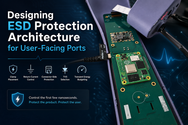
Designing for EMI From Day Zero: Certifiable Hardware and Designing ESD Protection Architecture for User-Facing Ports cover the two protection domains that most often fail certification late. Antenna Tuning in Small Enclosures for Wireless Performance is our field guide to matching RF inside a plastic housing. On power, Designing Redundant Power Inputs With Automatic Failover and Making Power Rails Self-Describing During Bring-Up cover sequencing and fault handling before firmware can help. Designing Sensor Boards That Don't Drift With Temperature and PCB Flex for Sensors: Designing Reliability Under Movement round out sensor integration under real environmental stress.
These are the notes we wish we'd had before the first prototype run — now public for whoever's fighting the same trade-offs.